


EDACafe Editorial Roberto Frazzoli
Roberto Frazzoli is a contributing editor to EDACafe. His interests as a technology journalist focus on the semiconductor ecosystem in all its aspects. Roberto started covering electronics in 1987. His weekly contribution to EDACafe started in early 2019. Optimizing RTL designs prior to implementation with Cadence Joules RTL Design StudioAugust 11th, 2023 by Roberto Frazzoli
A closer look at the new solution with the help of Rob Knoth, Product Management Group Director in the Digital & Signoff Group at Cadence With its recently announced “Joules RTL Design Studio”, Cadence is offering “a new solution that provides users with actionable intelligence to accelerate the register transfer level (RTL) design and implementation process.” According to Cadence, front-end designers can now access digital design analysis and debugging capabilities from a single, unified cockpit, enabling fully optimized RTL design prior to implementation handoff. For years, Cadence maintains, front-end designers have lacked visibility of RTL metrics on power, performance, area, and congestion (PPAC). Now, with the Joules RTL Design Studio, exploration and prototyping are possible prior to committing the design to the place and route phase. EDA News RoundupAugust 4th, 2023 by Roberto Frazzoli
Catching up on some of the news from the last thirty days or so, this week we will focus on some of the latest EDA announcements. Ansys’ 2023 R2 release, AnsysGPT, Ansys-Altium connection Recent announcements from Ansys include the introduction of its latest release, 2023 R2, and the limited beta release of AnsysGPT, a multilingual, conversational, AI virtual assistant for customer support. Developed using ChatGPT technology available via the Microsoft Azure OpenAI Service, AnsysGPT uses Ansys public data to answer technical questions concerning Ansys products, relevant physics, and engineering topics. Another recent announcement from the company concerns the digital connection of Altium’s electronic computer-aided design tools and Ansys simulation tools included in Ansys Electronics Desktop. Cadence’s Joules RTL Design Studio Cadence has announced its Joules RTL Design Studio, a new solution to accelerate the RTL design and implementation process. Front-end designers can access digital design analysis and debugging capabilities from a single, unified cockpit, which – according to the company – will enable fully optimized RTL design prior to implementation handoff. Users will also be able to leverage generative AI for RTL design exploration and big data analytics. According to Cadence, by enabling quick and accurate physical estimates, Joules RTL Design Studio can unlock up to 5X productivity and up to 25% quality of results (QoR) improvements in the RTL. Startup Nullspace offers over 25x faster EM simulation for antenna and radar designAugust 3rd, 2023 by Roberto Frazzoli
Flagship product of the new engineering software company – a spinoff from defense contractor IERUS Technologies – is an electromagnetic simulation software that has been tested on real-world antenna, microwave, and scattering problems for the last twelve years Wireless applications are getting ever more complex in several key industries such as defense, aerospace, 5G/6G communications, and automotive. Some of the design challenges concern multi- and wideband antennas, active and passive electronically steered arrays, MIMO antennas with complex beamforming, complex microwave networks, cosite interference when multiple antennas are placed on vehicles or aircrafts, and more. Companies developing advanced communication systems rely on electromagnetic simulation software that must combine speed, accuracy and flexibility, to reduce the development time while avoiding design errors.
Read the rest of Startup Nullspace offers over 25x faster EM simulation for antenna and radar design Special report: DAC and Semicon West 2023July 19th, 2023 by Roberto Frazzoli
Artificial intelligence, Moore’s law, chiplets, and High NA EUV were among the themes discussed by keynoters and panelists at the two industry events, both held in San Francisco from July 9-10 to July 13 Thousands of industry professionals and academic researchers involved in all different aspects of the semiconductor ecosystem gathered in San Francisco last week – either as attendees, exhibitors, presenters, or speakers – for the 2023 editions of the Design Automation Conference and Semicon West. Back to normal after the pandemic, the two co-located events offered a rich menu to the semiconductor community – combining research papers, exhibition floors, keynotes and panels. Adding to this offering, Semicon West was also co-located with the Flex event, and two European semiconductor research institutes – Belgium’s imec and France’s CEA-Leti – also organized their own forums at venues nearby (ITF Semicon USA and Leti Semicon Workshop, respectively). Here we will try to summarize some of the concepts that emerged from some of the keynotes and panels. EDA: no disruptions ahead Let’s start with EDA. Overall, it looks like the industry is not expecting any major disruptions on the short term. Artificial intelligence will obviously continue to play a key role in the evolution of EDA tools, but today this can be taken for granted and cannot be considered a new trend anymore. Part of the debate about EDA concerned the adaptation of existing EDA tools to the change of external conditions, such as the advent of cloud computing. The lack of disruptive innovations was effectively summarized by a rather provocative questions asked by Prit Banerjee, Ansys’ CTO, to EDA veterans Joe Costello and Wally Rhines during a panel. In short, Banerjee – speaking from the audience, not as a panelist – maintained that until now the major EDA vendors have just “tweaked” their EDA tools to adapt them to new technologies – such as parallel processing, AI, cloud computing – and asked if there is now space for a new EDA flow that is natively optimized for those new resources. Joe Costello answered that it’s a great idea, but today it would be difficult to find the money to undertake such an effort. Samsung Foundry EDA tool certifications; AMD’s new emulation FPGA; AMD gaining ground in AI trainingJuly 7th, 2023 by Roberto Frazzoli
Reportedly, the latest update on the U.S.-China tech fight is China’s decision to place exports restriction on gallium and germanium, which – according to some observers – could be followed by restrictions on rare earth exports. As for semiconductor subsidies updates, Broadcom will reportedly invest in a European Union-funded program in Spain which would include the construction of “large-scale back-end semiconductors facilities unique in Europe.” And French research institute CEA will receive funding from the French government for the construction of a new fab in Grenoble with the goal of downscaling FD-SOI (fully depleted silicon on insulator) chips below 10-nanometer and a to develop a new generation non-volatile onboard memory. Samsung Foundry roadmap updates On occasion of its recent Samsung Foundry Forum in San Jose, the South Korean company announced it will begin mass production of the 2-nanometer process for mobile applications in 2025, and then expand to HPC in 2026 and automotive in 2027. Mass production of SF1.4 will begin in 2027 as planned. From 2025, Samsung will begin foundry services for 8-inch gallium nitride power semiconductors. The 5-nanometer radio frequency process is also under development and will be available in the first half of 2025. Samsung Foundry is adding new manufacturing lines in Pyeongtaek, South Korea, and Taylor, Texas. The company said the construction of the new fab in Taylor is proceeding according to initial plans and is expected to finish by the end of the year, beginning operation in the second half of 2024. Among other news, Samsung is launching its ‘Multi-Die Integration Alliance’ in collaboration with partner companies and players in memory, substrate packaging, and testing. The MDI Alliance aims to create a packaging technology ecosystem for 2.5D and 3D heterogeneous integration. Intel’s new operating model; investments in India; Stellantis-Foxconn JV; a 51.2 Tbps SerDesJune 26th, 2023 by Roberto Frazzoli
A fund backed by the Japanese government has reportedly agreed to buy Japanese photoresists supplier JSR. The deal would represent an additional effort of the Japanese government to revitalize its domestic semiconductor industry. Among the other interesting news this week, Intel implicitly admitting (in this press release) that it is currently spending up to $1.5 billion per year due to operational inefficiencies that its competitors don’t have. This refers to expedited wafers and test times, as explained below. Intel to adopt an internal “fabless-foundry” model Intel will adopt a new operating model where its internal product groups will move to a foundry-style relationship with the company’s manufacturing group. In this new “internal foundry” model, Intel’s product business units will engage with the company’s manufacturing group in a similar fashion that fabless semiconductor companies engage with external foundries. Intel’s manufacturing groups will be accountable to a standalone profit and loss (P&L) for the first time. The company expects this change to boost efficiency and therefore deliver significant cost savings. One example concerns “expedited” wafers that business units decide to move through Intel’s manufacturing process, which are costly and reduce factory efficiency. Going forward, this service charge will be borne by the business units, and it’s expected that it will reduce the number of expedites “to be on par with the competition”. Another example concerns Intel’s test times, which currently run “double or triple those of competitors”. As business units are charged market prices based on test time, Intel expects pre-silicon design choices to reduce these test times. RF EDA updates; Samsung Foundry-IP vendors agreements; AMD’s AI products and strategy; Intel planning new EMEA facilitiesJune 19th, 2023 by Roberto Frazzoli
In view of its upcoming IPO, Arm is reportedly looking for some “anchor investors” among its main customers and end users. Companies in talks with Arm include Intel, Alphabet, Apple, Microsoft, TSMC, and Samsung. Let’s now move to this week’s news roundup, which mostly concerns EDA and IP. Among the other news, AMD disclosing details about its artificial intelligence products and strategy. RF EDA updates: Keysight, Xpeedic Keysight has introduced a new release of its PathWave Advanced Design System. The ADS 2024 suite offers new millimeter wave and subterahertz frequency capabilities targeting 5G and future 6G chips. According to Keysight, 3D electromagnetic analysis can be accelerated thanks to next-generation solvers, application-aware meshing algorithms, and an innovative circuit co-design and simulation approach. Increased circuit designer productivity is achieved through enhancements to the RFPro tool, which streamlines monolithic microwave integrated circuit and module workflows. Performance for microwave power amplifier designs can also be improved thanks to electrothermal simulation, signal modulation, and analysis capabilities. Xpeedic, too, has recently unveiled a new edition of its RF EDA solution. Innovations concern XDS, Xpeedic’s RF system-level design and simulation platform; IRIS, its on-chip passive modeling and simulation tool; and iModeler, a passive model generation tool. More semi subsidies; Intel’s BPD advancements; qualities of GeSn alloy; EV charging defacto standardJune 12th, 2023 by Roberto Frazzoli
Updates concerning automotive applications make up a significant part of this week’s news roundup. Among the other themes, backside power delivery is getting closer to real-life applications; and more subsidies are going to benefit the European semiconductor ecosystem. More European subsidies In addition to the EU Chips Act, the European Union and some individual member States are going to provide more subsidies to their domestic semiconductor ecosystem. The European Commission has approved an “Important Project of Common European Interest” (‘IPCEI’) to support research, innovation and the first industrial deployment of microelectronics and communication technologies across the value chain. Fourteen member States will provide up to €8.1 billion in public funding, which is expected to unlock additional €13.7 billion in private investments. As part of this IPCEI, 56 companies, including small and medium-sized enterprises and start-ups, will undertake 68 projects. 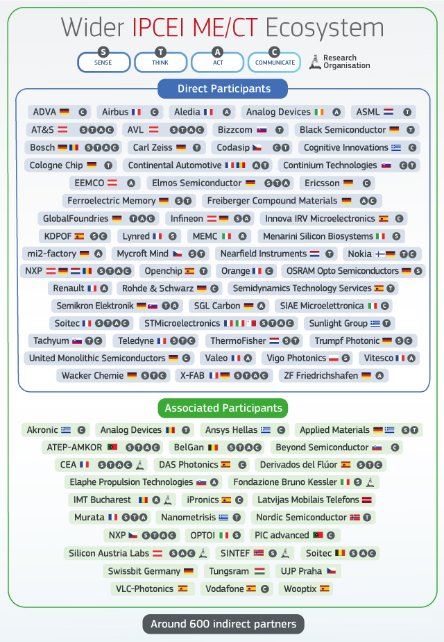 Source: European Commission Separately, the French government has announced it will provide 2.9 billion euros ($3.10 billion) in state aid to help support an investment of 7.5 billion euros that STMicroelectronics and GlobalFoundries are making to build a semiconductor factory in Crolles, France. Arm’s TCS23; AI partnerships; nickel aluminide; DVFS vulnerability; Cadence acquires PulsicJune 2nd, 2023 by Roberto Frazzoli
Open-source software for an open-source ISA: the Risc-V Software Ecosystem (RISE) Project is a new initiative dedicated to enabling a software ecosystem for application processors that includes software development tools, virtualization support, language runtimes, Linux distribution integration, and system firmware, working upstream first with existing open-source communities in accordance with open-source best practices. The RISE Governing Board includes Andes, Google, Intel, Imagination, MediaTek, Nvidia, Qualcomm, Red Hat, Rivos, Samsung, SiFive, T-Head, and Ventana. New Arm mobile computing platform At the recent Computex event in Taiwan, Arm announced its Total Compute Solutions 2023 (TCS23), a new platform for mobile computing aimed at premium smartphones. TCS23 IP includes a new Arm Immortalis GPU based on the 5th Generation GPU architecture, a new cluster of Armv9 CPUs supporting artificial intelligence, and other enhancements. A new graphics feature introduced in the 5th Gen GPU architecture is Deferred Vertex Shading (DVS), a technique that redefines the dataflow and enables partners to scale for larger core counts and higher performance points. A key part of the CPU cluster is the new Arm Cortex-X4 – “the fastest CPU that we have ever built,” Arm stated in a blog post – bringing 15 percent more performance compared to the Cortex-X3 while consuming 40 percent less power on the same process. Arm is taping out the Cortex-X4 on the TSMC N3E process. Cadence will support customers using the new Arm TCS23 through RTL-to-GDS digital flow Rapid Adoption Kits (RAKs) for 3nm and 5nm nodes. The company has fine-tuned its RAKs for Arm Cortex-X4, Cortex-A720 and Cortex-A520 CPUs and Immortalis-G720, Mali-G720 and Mali-G620 GPUs. Cadence verification flow has also been optimized for the newest Arm CPUs and GPUs. Synopsys, too, has announced support for TCS23 through QuickStart Implementation Kits (QIKs) that are tuned for the latest 5, 4 and 3nm process technologies. Nvidia approaching trillion-dollar valuation; Applied Materials’ “world’s largest” semi R&D facility; new Intel AI processorsMay 26th, 2023 by Roberto Frazzoli
According to Reuters, Nvidia is close to becoming the first trillion-dollar chip firm after its stock price increased about 25%, taking the company value to nearly $945 billion. The steep increase happened after Nvidia reportedly projected a quarterly revenue more than 50% above the average Wall Street estimate. “A trillion dollars of installed global data center infrastructure will transition from general purpose to accelerated computing as companies race to apply generative AI into every product, service and business process. (…) We are significantly increasing our supply to meet surging demand for them,” said Nvidia CEO Jensen Huang in a press release announcing the company’s latest financial results. AI Generated Silicon Design Challenge And one of the processes to which generative AI could be applied is chip design, at least according to Efabless which has just announced its “AI Generated Open-Source Silicon Design Challenge”. According to the company, Generative AI offers the potential to revolutionize chip design by automating many of the time-consuming tasks involved in the process. In this challenge, participants will use generative AI (e.g. chatGPT, Bard or similar) to generate Verilog from natural language prompts. Here’s a video example. The designs will then be implemented using the Efabless chipIgnite platform, which includes an SoC template (Caravel) providing rapid chip-level integration, and an open-source RTL-to-GDS digital design flow (OpenLane). Efabless intends to manufacture at least three winning designs. |
|
|
|||||
|
|
|||||
|
|||||


 Animation, 3D Art and 3D Models")