


EDACafe Editorial Roberto Frazzoli
Roberto Frazzoli is a contributing editor to EDACafe. His interests as a technology journalist focus on the semiconductor ecosystem in all its aspects. Roberto started covering electronics in 1987. His weekly contribution to EDACafe started in early 2019. Nvidia approaching trillion-dollar valuation; Applied Materials’ “world’s largest” semi R&D facility; new Intel AI processorsMay 26th, 2023 by Roberto Frazzoli
According to Reuters, Nvidia is close to becoming the first trillion-dollar chip firm after its stock price increased about 25%, taking the company value to nearly $945 billion. The steep increase happened after Nvidia reportedly projected a quarterly revenue more than 50% above the average Wall Street estimate. “A trillion dollars of installed global data center infrastructure will transition from general purpose to accelerated computing as companies race to apply generative AI into every product, service and business process. (…) We are significantly increasing our supply to meet surging demand for them,” said Nvidia CEO Jensen Huang in a press release announcing the company’s latest financial results. AI Generated Silicon Design Challenge And one of the processes to which generative AI could be applied is chip design, at least according to Efabless which has just announced its “AI Generated Open-Source Silicon Design Challenge”. According to the company, Generative AI offers the potential to revolutionize chip design by automating many of the time-consuming tasks involved in the process. In this challenge, participants will use generative AI (e.g. chatGPT, Bard or similar) to generate Verilog from natural language prompts. Here’s a video example. The designs will then be implemented using the Efabless chipIgnite platform, which includes an SoC template (Caravel) providing rapid chip-level integration, and an open-source RTL-to-GDS digital design flow (OpenLane). Efabless intends to manufacture at least three winning designs.
Applied Materials to build a large Silicon Valley facility The US “CHIPS and Science Act”, a subsidy plan aimed at supporting the domestic semiconductor industry, has sparked another initiative. Applied Materials has announced incremental capital investments of up to $4 billion over the next seven years to build “the world’s largest and most advanced facility for collaborative semiconductor process technology and manufacturing equipment research and development.” Named “Equipment and Process Innovation and Commercialization” (EPIC) Center, the facility will be located at an Applied campus in Silicon Valley and will include more than 180,000 square feet (over 16,000 square meters) of state-of-the-art cleanroom. The collaborative aspect of the initiative refers to the fact that chipmakers will be able to have their own dedicated space within the facility, extending their in-house pilot lines and providing early access to next-generation technologies and tools – months or even years before equivalent capabilities can be installed at their own premises. Collaboration with universities is also part of the project, as academic researchers will be granted access to the full range of industrial-scale capabilities to validate their ideas. The innovation center is expected to be completed by early 2026. The scale of Applied’s investment is contingent upon receiving support from the U.S. government through provisions of the CHIPS and Science Act. Broadcom to develop components for Apple In a move that seems to be linked with the current geopolitical tensions and de-globalization trends, Apple has announced a new multiyear, multibillion-dollar agreement with Broadcom. Through this collaboration, Broadcom will develop 5G radio frequency components — including FBAR filters — and advanced wireless connectivity components. The FBAR filters will be designed and built in several key American manufacturing and technology hubs, including Fort Collins, Colorado, where Broadcom has a major facility. “We’re thrilled to make commitments that harness the ingenuity, creativity, and innovative spirit of American manufacturing,” said Tim Cook, Apple’s CEO. “All of Apple’s products depend on technology engineered and built here in the United States, and we’ll continue to deepen our investments in the U.S. economy because we have an unshakable belief in America’s future.” Intel’s upcoming AI processors At the ISC High Performance Conference recently held in Hamburg, Germany, Intel provided product roadmap updates about Granite Rapids, a next-generation CPU to address memory bandwidth demands, and Falcon Shores, a GPU aimed at a diverse set of workloads for HPC and AI. Granite Rapids will employ a new type of DIMM – Multiplexer Combined Ranks (MCR) – which achieves speeds of 8,800 megatransfers per second based on DDR5 and greater than 1.5 terabytes/second (TB/s) of memory bandwidth capability in a two-socket system. Falcon Shores GPU will offer the flexibility to implement system-level CPU and discrete GPU combinations to adapt to fast-changing workloads. Based on a modular, tile-based architecture, the new GPU will support data types from FP64 to BF16 to FP8; enable up to 288GB of HBM3 memory with up to 9.8TB/s total bandwidth; empower the CXL programming model; and present a unified GPU programming interface through oneAPI. Intel’s FPGA offer PCIe 5.0 and CXL capabilities Another recent Intel announcement concerns the Agilex 7 FPGA equipped with the R-Tile chiplet, which is now production-qualified and shipping in volume. Agilex 7 FPGAs are built with a heterogeneous multi-die architecture, with an FPGA fabric chiplet in the center connected to transceiver chiplets via Intel’s embedded multi-die interconnect bridge (EMIB) technology. The R-Tile, in particular, is a chiplet that provides hard-IP blocks for PCIe 5.0 and CXL capabilities. These high bandwidth FPGAs are intended to work as accelerators – offloading tasks from the host CPU in cloud computing and HPC applications. 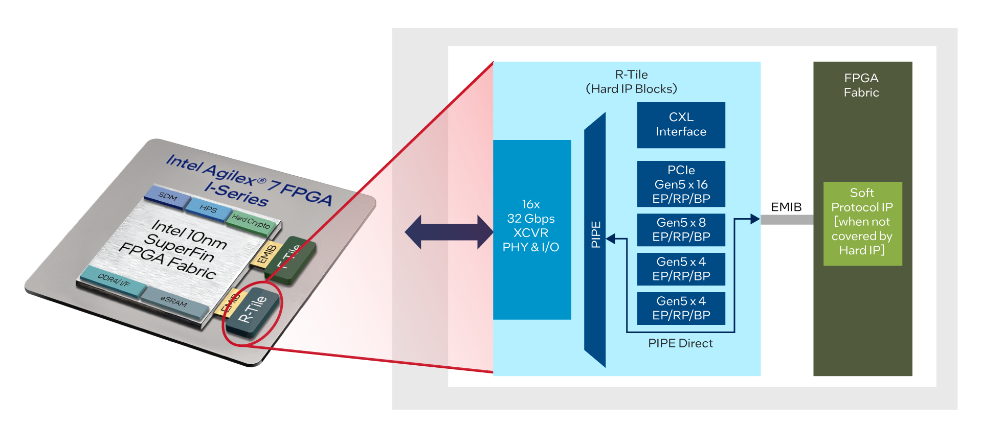 Credit: Intel Eliyan’s chiplet interconnect technology achieves first silicon Also related to the chiplet trend, Eliyan has recently announced first silicon availability for its NuLink PHY chiplet interconnect technology, achieved in one year from company’s initial funding. Implemented in a standard 5-nanometer process from TSMC, the chip operates at 40Gbps/bump delivering over 2.2Tbps/mm of beachfront bandwidth at 130um pitch on standard organic packaging. According to Eliyan, the successful silicon implementation demonstrates that NuLink PHY technology in standard organic packaging achieves similar bandwidth, power efficiency, and latency as die-to-die implementations using advanced packaging technologies, but without the drawbacks of those complex and expensive solutions. Axiado trusted control/compute units Axiado has introduced the AX3000 and AX2000 trusted control/compute units (TCUs), what the company claim are “the world’s first fully integrated AI-driven hardware security platform solutions”. The processors are designed to help detect cybersecurity and ransomware attacks on servers and infrastructure elements in cloud datacenters, 5G networks, and network switches. According to the company, the Axiado AX3000/AX2000 TCUs represent a new category of forensic-enabled cybersecurity processors that are designed to enhance existing Zero-Trust models. TCUs combine silicon, AI and data collection, and software. The solutions are compliant with Open Compute Project’s approved Datacenter Secure Control Module Specification (DC-SCM). Further reading Microsoft Build, the company’s annual flagship event for developers, took place from May 23 to 25. Here is a summary of all the announcements that Microsoft made at the conference. Reconnecting to the opening theme of this week’s news roundup, let’s finish by noting that – according to market intelligence firm CB Insights – generative AI has already produced thirteen “unicorns” (startups valued at over $1 billion). Across these companies, the average time to reach unicorn status is 3.6 years but for the unicorn club as a whole the average is 7 years — almost twice as long. 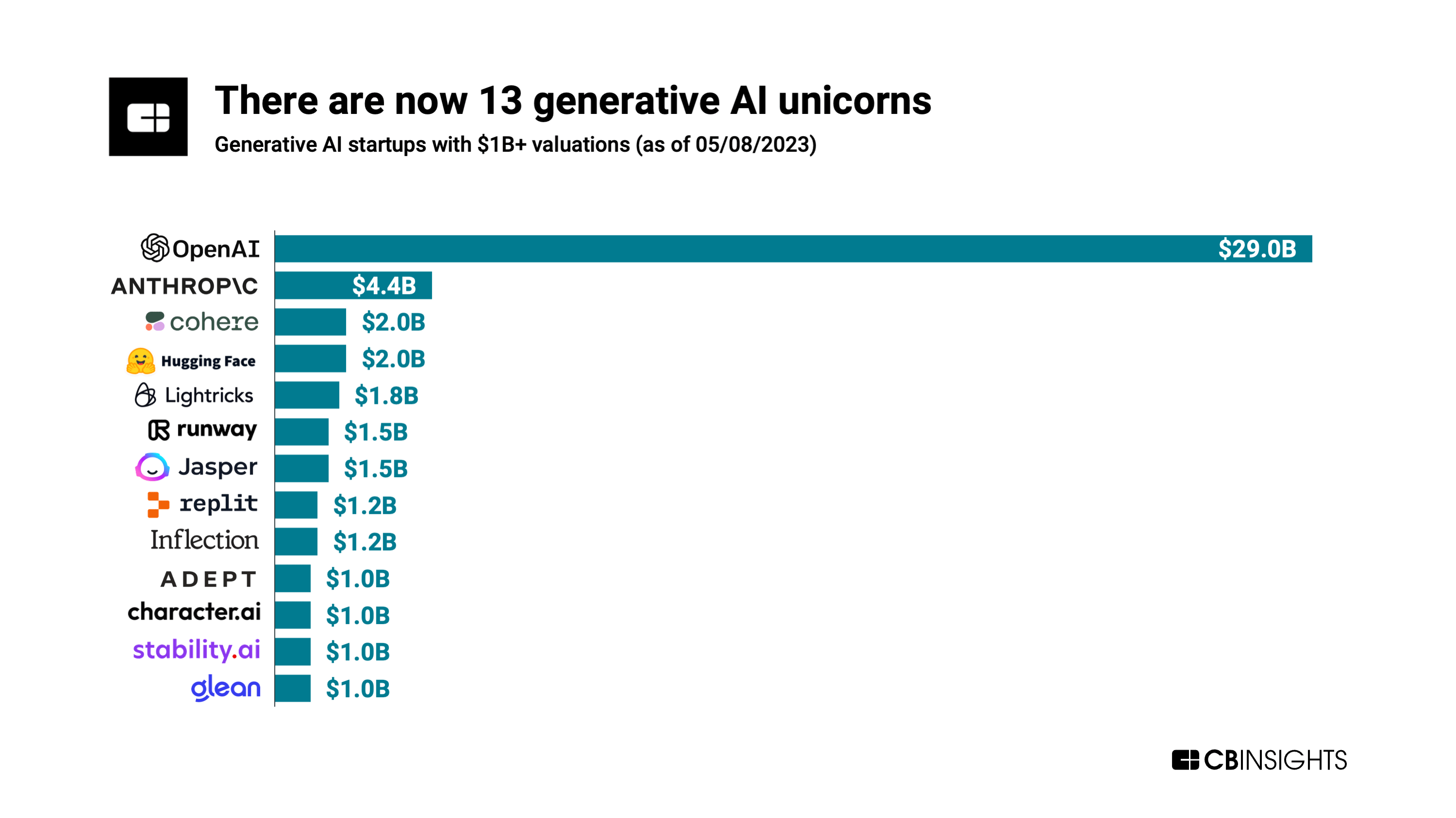 Credit: CB Insights |
|
|
|||||
|
|
|||||
|
|||||


 Animation, 3D Art and 3D Models")