Roberto Frazzoli Roberto Frazzoli is a contributing editor to EDACafe. His interests as a technology journalist focus on the semiconductor ecosystem in all its aspects. Roberto started covering electronics in 1987. His weekly contribution to EDACafe started in early 2019.
Innovations from the 2024 TSMC Technology Symposium
May 20th, 2024 by Roberto Frazzoli
The European edition of TSMC’s 2024 Technology Symposium – held in Amsterdam on May 14 – allowed EDACafe to gain some additional insights on the innovations that the Taiwan-headquartered foundry first announced on April 24 at the North America edition of the event. Besides providing a roadmap of new opportunities for chipamkers and OEMs, these innovations also shed some light on the strategies that TSMC is planning to pursue over the next few years to retain its world-leading role.
TSMC’s CEO C.C. Wei on stage in Amsterdam. Credit: TSMC
Entering “the Angstrom era” with the A16 process
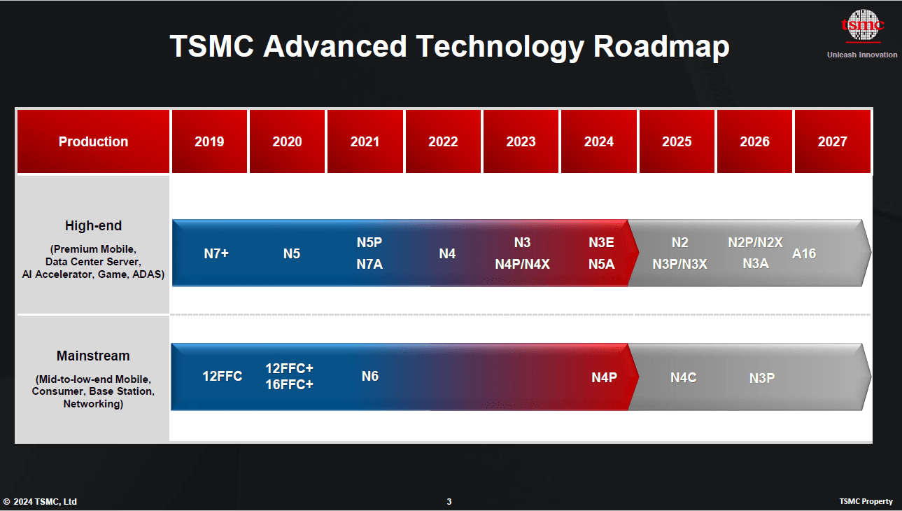
Among TSMC’s most notable announcements is the upcoming nanosheet-based A16 process, where A clearly stands for Angstrom. Always keeping in mind what IEEE says about process names (i.e. that today they are just marketing labels, with no connection to the real size of transistor features), it’s inevitable to compare TSMC’s A16 process with Intel’s 18A process, and the difference in numbers – 16 vs 18 – suggests that the Taiwanese foundry hopes to leapfrog competitors even in the Angstrom era. According to the figures released by TSMC, the new A16 process – in comparison to the company’s N2P – will provide 8-10% speed improvement at the same Vdd (positive power supply voltage), 15-20% power reduction at the same speed, and up to 1.10X chip density improvement for data center products. The impact of these achievements can be significant considering large datacenters, where a 20% power reduction translates into a big amount of energy in absolute terms. TSMC’s A16 process is best suited for HPC products and is planned to enter production in 2026. As for moving existing designs to the new process, 86% of standard cells can be ported directly from N2P to A16, whereas 16% need a re-optimization.
Credit: TSMC
TSMC’s approach to backside power delivery
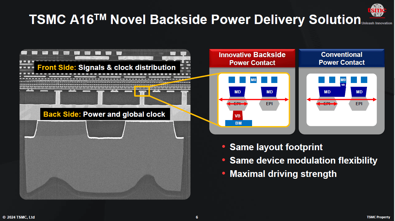
It looks like the key to the PPA improvements achieved by TSMC’s A16 process is the adoption of backside power delivery. Moving power routing to the back side of the chip enables the new technology to save space on the front side and to shorten power paths, thus reducing IR drops and parasitics. Intel was first to adopt backside power delivery, which is a general trend in the industry. However, TSMC’s Senior Vice President Kevin Zhang underlined the differences and advantages of TSMC’s approach. Called “Super Power Rail”, the new solution provides power to the transistors by reaching them directly through a contact from the back side of the die – instead of using a hole from the front side, as in the conventional schemes. According to TSMC, the novel backside power delivery solution preserves gate density and device width flexibility. Thermal management, however, becomes a critical aspect, as backside power delivery requires a very thin die, which can cause hotspots.
Credit: TSMC
High-NA EUV? Not yet
Even for its A16 process, TSMC will continue to use its existing EUV lithography equipment. The company is not planning to adopt high-NA tools, yet. Among many other aspects, the approach to high-NA EUV marks a sharp difference between TSMC and Intel Foundry. Notoriously, Intel Foundry has already purchased high-NA EUV tools for manufacturing purposes – not just for R&D – and is reportedly planning to use Direct Self-Assembly to make this technology cost-effective compared to double patterning with the conventional EUV tools. TSMC, in contrast, has chosen a more conservative approach, and is explaining it with the need to offer customers the best price-performance ratio. “I like the high-NA capabilities, but I don’t like the sticker price”, said Kevin Zhang. While it’s no surprise for an incumbent (TSMC) and for a challenger (Intel Foundry) to adopt different strategies, some questions remain unanswered. On the one hand, a financially healthy TSMC deems high-NA EUV tools too expensive at the moment; on the other hand, Intel Foundry – which just recently disclosed a 2023 operating loss of $7 billion – has cheerfully celebrated the purchase of the first high-NA piece of equipment, despite the price tag.
High quality home-made pellicles
One possible answer lies in the prowess that TSMC has gained in using their existing EUV lithography equipment. Jun He – TSMC’s Vice President, Quality & Reliability and Operations / Advanced Packaging Technology and Service – pointed out that TSMC was the first foundry to use EUV in volumes, and currently owns 56% of EUV equipment world installed base. The speaker also underlined that since 2019 TSMC has doubled the “wafer per day per tool” throughput and reduced 10x the reticle particle contamination. Key to these achievements, Jun He pointed out, is the quality level reached by TSMC’s home-made mask pellicles. According to the speaker, TSMC’s pellicles offer 4.5x more output, 80x less defectivity and 4x longer lifespan than commercial pellicles. This clearly has an impact on the equipment productivity, by reducing the need for servicing. TSMC has also been able to significantly reduce the power consumption of EUV lithography equipment. Will the foundry ever share its secrets with ASML?
Two different sizes for N2 standard cells
As for the N2 process – which is on track for production in the second half of 2025 – TSMC introduced a solution called NanoFlex, where Nano refers to nanosheet transistors. NanoFlex enables designers to choose between two different standard cell sizes, thanks to device width modulation. Short cells emphasize small area and greater power efficiency, while tall cells maximize performance. Designers can optimize the combination of short and tall cells within the same design block, tuning their designs to reach the optimal power, performance, and area tradeoffs for their application. According to TSMC, with selective use of tall cells, speed improves by 15% while keeping area and power efficiency intact. TSMC’s N3 process – which uses FinFETs – offers a similar option called FinFlex, where the power vs speed tuning is obtained by changing the number of transistor fins.
The European edition of the Symposium was also used by TSMC to reiterate the other innovations already announced at the Santa Clara event on April 24. Among them the N4C process, an extension of N4P technology with up to 8.5% die cost reduction and low adoption effort, scheduled for volume production in 2025. According to TSMC, N4C offers area-efficient foundation IP and design rules that are fully compatible with the widely-adopted N4P, with better yield from die size reduction, providing a cost-effective option for value-tier products to migrate to the next advanced technology node from TSMC.
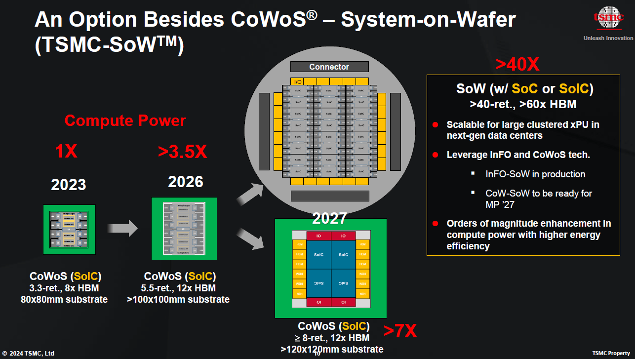
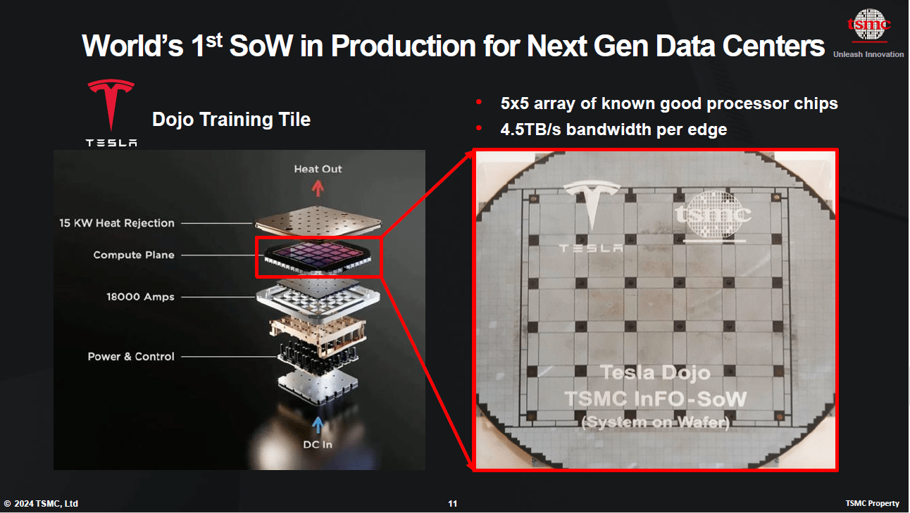
A new 3D packaging option: System-on-Wafer
Confirming the growing importance of advanced packaging technologies, TSMC devoted a significant part of the Symposium to its innovations in this area. Among them, the new System-on-Wafer solution enables to place a large array of dies on a 300-millimeter wafer. According to the company, this solution offers more compute power while occupying far less data center space and boosts performance per watt by orders of magnitude. TSMC’s first SoW offering, a logic-only wafer based on Integrated Fan-Out (InFO) technology, is already in production for Tesla. A chip-on-wafer version leveraging CoWoS technology is scheduled to be ready in 2027, enabling integration of SoIC, HBM and other components to create a wafer-level system with computing power comparable to a data center server rack, or even an entire server.
Credit: TSMC
Credit: TSMC
Packaging updates
At the Symposium, TSMC also provided updates and roadmaps for its existing advanced packaging solutions. The bumpless SoIC-X schemes for 3D chiplet stacking will evolve from the 9um bond pitch in front-to-back scheme available today to 3um pitch in front-to-front available in 2027. TSMC expects SoIC-X to achieve 30 customer tape-outs by the end of 2026. As for CoWoS, the company plans to develop an 8X reticle size version of this technology featuring A16 SoIC chips and twelve HBMs for production in 2027. The company will have enabled more than 150 CoWoS tapeouts for more than twenty-five customers by the end of this year. TSMC also stressed that the Nvidia Blackwell AI accelerator is the world’s first CoWoS-L product in volume production, integrating two N5 SoCs and eight HBM stacks in a module.
Additional packaging updates include the development of InFO-oS and CoWoS-R solutions for automotive applications such as ADAS, vehicle control, and vehicle central computers, targeting AEC-Q100 Grade 2 qualification by fourth quarter of 2025. Chiplets will enable automakers to differentiate their solutions for the various car models.
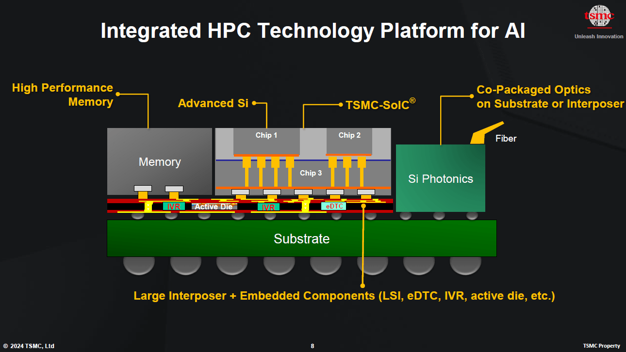
An electrical die and a photonic die in the same package
Another significant innovation announced by TSMC in this area is the Compact Universal Photonic Engine (COUPE) technology, which uses SoIC-X chip stacking technology to stack an electrical die on top of a photonic die. According to the company, the solution offers the lowest impedance at the die-to-die interface and higher energy efficiency than conventional stacking methods. TSMC plans to qualify COUPE for small form factor pluggables in 2025, followed by integration into CoWoS packaging as co-packaged optics (CPO) in 2026, bringing optical connections directly into the package.
Photonics as part of a complex packaging solution for HPC. Credit: TSMC
A glimpse into the future: CFET devices, metallization improvements
TSMC’s R&D resources are already investigating future technologies beyond nanosheet transistors. Just like most of the semiconductor industry, the Taiwan-headquartered foundry considers CFET – a solution based on vertically stacking an nFET and a pFET – a likely scaling candidate. According to TSMC’s estimates, CFET density gain would fall between 1.5 to 2X after factoring in routing and process complexity. TSMC is also planning to introduce new interconnect technologies to improve interconnect performance. Innovations will include a new via scheme for copper-based interconnect to reduce via resistance by another 25%; a new via etch-stop-layer to lower coupling capacitance by approximately 6%; a new barrier for copper that can reduce copper line resistance by approximately 15%; a new metal material with air-gap, which could slash coupling capacitance by approximately 25%; the use of intercalated graphene to dramatically reduce interconnect delays.
Boosting capacity
Fab capacity is a key issue in the AI era. As for advanced packaging, TSMC is boosting its SoIC and CoWoS production capacity at expected CAGRs of over 100% and over 60%, respectively. TSMC’s effort to boost capacity was underlined by Jun He, who also noted that the company has recently accelerated the construction of new fabs. As Kevin Zhang pointed out, for the first time in TSMC’s history some of the new fabs are devoted to specialty technologies – an umbrella term covering Ultra Low Power, MRAM, RRAM, BCD, RF etc. Specialty fabs will be built in Nanjing, Kumamoto and Dresden. And speaking of Dresden, Germany, TSMC unveiled the logo of its European venture ESMC, which – in collaboration with Bosch, Infineon and NXP – will offer N28 and N16 process technologies.
The ESMC logo. Credit: TSMC
This entry was posted
on Monday, May 20th, 2024 at 11:26 pm.
You can follow any responses to this entry through the RSS 2.0 feed.
You can leave a response, or trackback from your own site.


 Animation, 3D Art and 3D Models")