


EDACafe Editorial Roberto Frazzoli
Roberto Frazzoli is a contributing editor to EDACafe. His interests as a technology journalist focus on the semiconductor ecosystem in all its aspects. Roberto started covering electronics in 1987. His weekly contribution to EDACafe started in early 2019. More semi subsidies; Intel’s BPD advancements; qualities of GeSn alloy; EV charging defacto standardJune 12th, 2023 by Roberto Frazzoli
Updates concerning automotive applications make up a significant part of this week’s news roundup. Among the other themes, backside power delivery is getting closer to real-life applications; and more subsidies are going to benefit the European semiconductor ecosystem. More European subsidies In addition to the EU Chips Act, the European Union and some individual member States are going to provide more subsidies to their domestic semiconductor ecosystem. The European Commission has approved an “Important Project of Common European Interest” (‘IPCEI’) to support research, innovation and the first industrial deployment of microelectronics and communication technologies across the value chain. Fourteen member States will provide up to €8.1 billion in public funding, which is expected to unlock additional €13.7 billion in private investments. As part of this IPCEI, 56 companies, including small and medium-sized enterprises and start-ups, will undertake 68 projects. 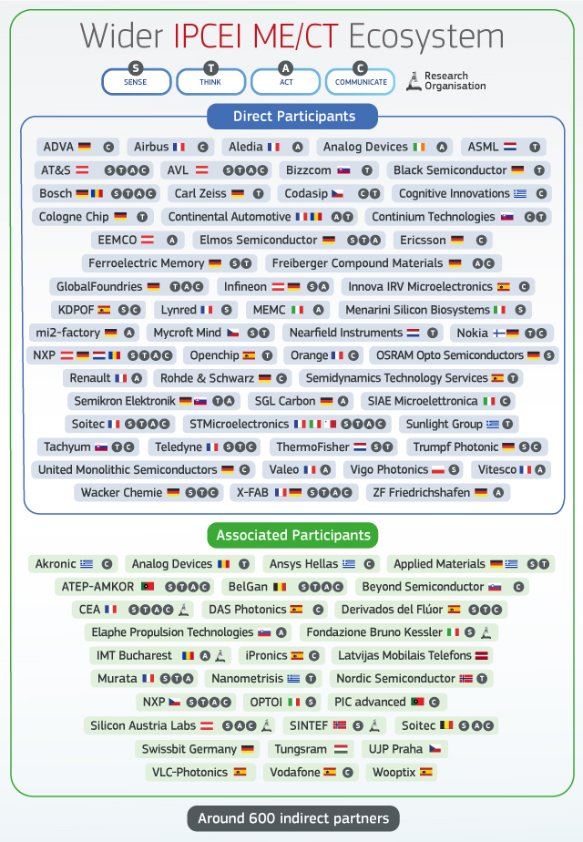 Source: European Commission Separately, the French government has announced it will provide 2.9 billion euros ($3.10 billion) in state aid to help support an investment of 7.5 billion euros that STMicroelectronics and GlobalFoundries are making to build a semiconductor factory in Crolles, France. Arm’s TCS23; AI partnerships; nickel aluminide; DVFS vulnerability; Cadence acquires PulsicJune 2nd, 2023 by Roberto Frazzoli
Open-source software for an open-source ISA: the Risc-V Software Ecosystem (RISE) Project is a new initiative dedicated to enabling a software ecosystem for application processors that includes software development tools, virtualization support, language runtimes, Linux distribution integration, and system firmware, working upstream first with existing open-source communities in accordance with open-source best practices. The RISE Governing Board includes Andes, Google, Intel, Imagination, MediaTek, Nvidia, Qualcomm, Red Hat, Rivos, Samsung, SiFive, T-Head, and Ventana. New Arm mobile computing platform At the recent Computex event in Taiwan, Arm announced its Total Compute Solutions 2023 (TCS23), a new platform for mobile computing aimed at premium smartphones. TCS23 IP includes a new Arm Immortalis GPU based on the 5th Generation GPU architecture, a new cluster of Armv9 CPUs supporting artificial intelligence, and other enhancements. A new graphics feature introduced in the 5th Gen GPU architecture is Deferred Vertex Shading (DVS), a technique that redefines the dataflow and enables partners to scale for larger core counts and higher performance points. A key part of the CPU cluster is the new Arm Cortex-X4 – “the fastest CPU that we have ever built,” Arm stated in a blog post – bringing 15 percent more performance compared to the Cortex-X3 while consuming 40 percent less power on the same process. Arm is taping out the Cortex-X4 on the TSMC N3E process. Cadence will support customers using the new Arm TCS23 through RTL-to-GDS digital flow Rapid Adoption Kits (RAKs) for 3nm and 5nm nodes. The company has fine-tuned its RAKs for Arm Cortex-X4, Cortex-A720 and Cortex-A520 CPUs and Immortalis-G720, Mali-G720 and Mali-G620 GPUs. Cadence verification flow has also been optimized for the newest Arm CPUs and GPUs. Synopsys, too, has announced support for TCS23 through QuickStart Implementation Kits (QIKs) that are tuned for the latest 5, 4 and 3nm process technologies. Nvidia approaching trillion-dollar valuation; Applied Materials’ “world’s largest” semi R&D facility; new Intel AI processorsMay 26th, 2023 by Roberto Frazzoli
According to Reuters, Nvidia is close to becoming the first trillion-dollar chip firm after its stock price increased about 25%, taking the company value to nearly $945 billion. The steep increase happened after Nvidia reportedly projected a quarterly revenue more than 50% above the average Wall Street estimate. “A trillion dollars of installed global data center infrastructure will transition from general purpose to accelerated computing as companies race to apply generative AI into every product, service and business process. (…) We are significantly increasing our supply to meet surging demand for them,” said Nvidia CEO Jensen Huang in a press release announcing the company’s latest financial results. AI Generated Silicon Design Challenge And one of the processes to which generative AI could be applied is chip design, at least according to Efabless which has just announced its “AI Generated Open-Source Silicon Design Challenge”. According to the company, Generative AI offers the potential to revolutionize chip design by automating many of the time-consuming tasks involved in the process. In this challenge, participants will use generative AI (e.g. chatGPT, Bard or similar) to generate Verilog from natural language prompts. Here’s a video example. The designs will then be implemented using the Efabless chipIgnite platform, which includes an SoC template (Caravel) providing rapid chip-level integration, and an open-source RTL-to-GDS digital design flow (OpenLane). Efabless intends to manufacture at least three winning designs. Fab investments; silicon vs WBG materials; compressing simulation code; Ansys acquires DiakoptoMay 19th, 2023 by Roberto Frazzoli
Competition heats up for processors aimed at cloud computing. Ampere (Santa Clara, CA) has just introduced a new family of what it calls “cloud native processors”, with 192 custom designed Ampere cores and a number of features aimed at cloud usages like AI. More news this week include innovations from both industry and academia. New fab investments: Analog Devices in Europe, Micron in Japan Analog Devices will invest €630 million at its European regional headquarters in Limerick, Ireland, to build a new 45,000 sq-ft R&D and manufacturing facility which will focus on signal processing innovations. The new facility is expected to triple ADI’s European wafer production capacity. The investment is planned as part of a collaboration within the European Union’s Important Projects of Common European Interest on Microelectronics and Communication Technologies (IPCEI ME/CT) initiative, and is supported by the Irish Government. One year ago, Analog Devices announced a separate investment of €100 million in “ADI Catalyst” at its Limerick campus. Ireland is also home to ADI’s main European Research and Development Center. Micron Technology will be introducing EUV lithography to its Hiroshima (Japan) fab, to manufacture its next generation of DRAM, the 1-gamma (1γ) node. The company expects to ramp EUV into production on the 1-gamma node in Japan (as well as in Taiwan) from 2025 onwards. Micron will be the first semiconductor company to bring EUV technology to Japan for production, and expects to invest up to 500 billion yen in 1-gamma process technology over the next few years, with close support from the Japanese government. Microsoft-AMD collaboration; Google’s new cloud platform; memory price to decline; Synopsys acquires Silicon FrontlineMay 12th, 2023 by Roberto Frazzoli
EDA research is alive: the DAC 2023 technical program received a record high number of submissions. For the Research Track, the Conference’s Technical Program Committee reviewed 1,156 submitted research manuscripts and accepted 263 for presentation and publication. In addition, 269 Engineering Track submissions were reviewed with 71 accepted for presentation. Hyperscalers updates: Microsoft, Meta, Google Microsoft and AMD are reportedly collaborating on artificial intelligence chips. Unlike what one would expect, the AI processor design is being provided by Microsoft, not by AMD: it is the Athena chip that was in the news a couple of weeks ago. Microsoft is also reportedly providing financial support to bolster AMD’s AI efforts. Meta (Facebook) has reportedly hired an Oslo-based team (at least ten engineers) that until late last year was building artificial-intelligence networking technology at British AI chip unicorn Graphcore. According to Reuters, Graphcore closed its Oslo office as part of a broader restructuring announced in October last year. Among the many innovations introduced on occasion of the recent Google I/O event, Google Cloud has announced the private preview launch of the next-generation A3 GPU supercomputer for training and inference of generative AI and large language models. The A3 VMs combine Nvidia H100 Tensor Core GPUs and Google’s custom-designed 200 Gbps IPUs, with GPU-to-GPU data transfers bypassing the CPU host and flowing over separate interfaces from other VM networks and data traffic. This enables up to 10x more network bandwidth compared to Google’s A2 VMs. The A3 supercomputer’s scale provides up to 26 exaFlops of AI performance. Digitally wrapped analog IP; 3D DRAM; CHIPS Act and EDA; Python accelerationMay 5th, 2023 by Roberto Frazzoli
Arm has officially started the process that will lead to its IPO on Nasdaq. As stated in a press release, the size and price range for the proposed offering have yet to be determined. Let’s now move to the rest of our weekly news roundup. Market numbers: semiconductors 1Q2023, EDA 4Q2022 The chip market is slowing down. According to the Semiconductor Industry Association (SIA), worldwide sales of semiconductors totaled $119.5 billion during the first quarter of 2023, a decrease of 8.7% compared to the fourth quarter of 2022 and 21.3% less than the first quarter of 2022. Sales for the month of March 2023, however, increased 0.3% compared to February 2023. The EDA market, in contrast, is doing well. As recently announced by the ESD Alliance, Electronic System Design industry revenue increased 11.3% from $3,468.2 million in the fourth quarter of 2021 to $3,858.7 million in the fourth quarter of 2022. Smartphone chipmakers seeking diversification In terms of chip demand, one of the market segments that are suffering is smartphones, and this is having an impact on the leading smartphone chip suppliers. Qualcomm’s shares reportedly sank 7%, over the past few days, after the company signalled it would take longer for the smartphone market to rebound from a post-pandemic slump. Qualcomm, however, is diversifying towards automotive and IoT application, and its automotive revenue grew 20% from Q2 2022 to Q2 2023. A similar diversification strategy is being pursued by MediaTek: “We are definitely moving our resources very, very rapidly toward the automotive and computing area because those areas will provide our growth in the next three to five years in the future,” said MediaTek’s CEO Rick Tsai during the 1Q23 earnings call. Read the rest of Digitally wrapped analog IP; 3D DRAM; CHIPS Act and EDA; Python acceleration AI-based PCB design; SerDes and UCIe advancements; fully configurable Risc-V cores; Arm’s own silicon chipApril 28th, 2023 by Roberto Frazzoli
Catching up on some of the news from the past few weeks, let’s start by noting that yet another hyperscaler is developing its own AI chip: according to press reports, Microsoft is working on a device code-named Athena, currently being tested. Microsoft is reportedly accelerating the rollout following the success of ChatGPT. Cadence leverages AI and the cloud to speed up PCB design The new Cadence Allegro X AI technology promises to reduce the time for PCB placement and routing tasks from days to minutes, and with equivalent or higher quality compared with manually designed boards. Reduction in design turnaround time is achieved by automating placement, metal pouring and critical net routing – leveraging a scalable architecture that uses compute infrastructure on the cloud. Placement automation using generative AI enables feasibility analysis in the early phases of design. Exploring a much larger solution space than what is possible through manual methods, the technology drives optimization of metrics such as shorter wire lengths while adhering to the design constraints. Integration with signal integrity and power integrity analysis through the Allegro X Platform enables the user to optimize the designs for electrical and thermal performance. According to Cadence, the solution achieves a 10X or more reduction in PCB design turnaround time. Special Report: Present and Future of the EDA Oligopoly – Part TwoApril 27th, 2023 by Roberto Frazzoli
Will the market dominance of EDA’s “big three” remain immune from the new factors that are impacting the semiconductor ecosystem? We tried to answer this question with the help of Laurie Balch (Pedestal Research), Harry Foster (Siemens EDA), David Kanter (MLCommons), KT Moore (Cadence), Wally Rhines (Cornami) In Part One of this special report we focused on the factors of stability that have contributed to the creation of the EDA oligopoly (Cadence, Siemens EDA and Synopsys, of course) and still underpin the incumbents’ market dominance: a certain degree of complementarity among the ‘big three’ product offerings, and the high cost incurred by customers if they want to switch from one EDA vendor to another. We also examined the overall performance of EDA solutions for IC/ASIC design through the findings of the 2022 Wilson Research Group Functional Verification Study, which shows – on average – a 24 percent rate of first silicon success and a 33 percent rate of project completion without schedule slips. Additionally, we discussed the attitude of the EDA industry towards benchmarking and open-source tools. In this second part of our report we will address some of the criticisms that have been raised against the EDA oligopoly and will consider some potential factors of change. We will do that, again, through interviews with EDA professionals (Harry Foster, Chief Scientist Verification at Siemens EDA; KT Moore, VP of corporate marketing at Cadence; Wally Rhines, CEO at Cornami and formerly CEO at Mentor Graphics for twenty-four years), an EDA market analyst (Laurie Balch, Research Director at Pedestal Research) and an executive from a benchmarking consortium (David Kanter, Executive Director at MLCommons). A different view on the EDA status quo: DARPA and the OpenRoad project Is the vendor oligopoly a positive or a negative thing for the EDA users? Over the past few years, DARPA (Defense Advanced Research Projects Agency) has often expressed opinions that are relevant for a discussion on this topic. In particular, the EDA theme has been addressed by Serge Leef when he was Program Manager of the DARPA’s Microsystems Technology Office. Other relevant concepts can be found in the OpenRoad project lead by Professor Andrew Kahng from UC San Diego, one of the open-source EDA initiatives supported by DARPA. Unfortunately, neither Serge Leef – who left DARPA last year – nor any other DARPA spokesperson, nor Professor Kahng could be reached for comments, so here we will refer to documents that are publicly available online. Read the rest of Special Report: Present and Future of the EDA Oligopoly – Part Two Special Report: Present and Future of the EDA Oligopoly – Part OneApril 25th, 2023 by Roberto Frazzoli
Will the market dominance of EDA’s “big three” remain immune from the new factors that are impacting the semiconductor ecosystem? We tried to answer this question with the help of Laurie Balch (Pedestal Research), Harry Foster (Siemens EDA), David Kanter (MLCommons), KT Moore (Cadence), Wally Rhines (Cornami) The global EDA market is notoriously dominated by just three U.S.-based major vendors: Cadence, Siemens EDA and Synopsys, of course. This status quo has been stable for decades; will it continue to be this stable in the future? Several new events and trends have recently started impacting the semiconductor ecosystem: US-China tensions, the AI boom, the growth of hyperscalers, massive subsidies supporting the construction of new fabs around the world etc. Will any of these new events have an impact on the EDA oligopoly? We tried to answer this question by interviewing EDA professionals (Harry Foster, Chief Scientist Verification at Siemens EDA; KT Moore, VP of corporate marketing at Cadence; Wally Rhines, CEO at Cornami and formerly CEO at Mentor Graphics for twenty-four years), an EDA market analyst (Laurie Balch, Research Director at Pedestal Research) and an executive from a benchmarking consortium (David Kanter, Executive Director at MLCommons, whose contribution will be featured in the next part of this report). In this first part, we will delve deeper into the factors of stability that have contributed to the creation of the oligopoly and still underpin the incumbents’ market dominance. Adding to the description of the status quo, we will also focus on the overall performance of EDA solutions, as well as on the attitude of the EDA industry towards benchmarking and open-source tools. The second part of our report will address some of the criticisms that have been raised against the EDA oligopoly and will consider some potential factors of change. Read the rest of Special Report: Present and Future of the EDA Oligopoly – Part One AI-based macro placement; open-use LLMs; new silicon-compatible materials for AI applicationsMarch 30th, 2023 by Roberto Frazzoli
Artificial intelligence is the common underlying theme for most of this week’s updates. Among them, Nvidia is in the news with an EDA research work, after last week announcement concerning its solution for computational lithography – the last software step before mask production. Nvidia research on AI-based macro placement At the recent ISPD (International Symposium on Physical Design), a group of Nvidia researchers presented a paper on AI-based macro placement. The paper proposes AutoDMP, a methodology that leverages DREAMPlace, a preexisting open-source GPU-accelerated placer, to place macros and standard cells concurrently in conjunction with automated parameter tuning using a multi-objective hyperparameter optimization technique. As a result, the team could generate high-quality predictable solutions, improving the macro placement quality of academic benchmarks compared to baseline results generated from academic and commercial tools. According to the Nvidia researchers, AutoDMP is also computationally efficient, optimizing a design with 2.7 million cells and 320 macros in three hours on a single Nvidia DGX Station A100. The key contributions of the work include using multi-objective Bayesian optimization to search the design space of macro placements, targeting three PPA proxy objectives post-place: wirelength, cell density, and congestion; using a two-level PPA evaluation scheme to manage the complexity of the search space; and enhancing the DREAMPlace placer. Open-source benchmarks used include Ariane, a single core Risc-V CPU; the MemPool Group and BlackParrot designs, many-core Risc-V CPUs with large amounts of on-chip SRAMs; and an NVDLA partition. A previous research work on AI-based macro placement, from Google, had been criticized for not providing enough publicly available data and for comparing the AI performance to an unspecified human expert’s performance. The new Nvidia work seems to be able to withstand these types of criticism, as it includes details on benchmarking and compares the AI performance with a commercial EDA tool, Cadence Innovus. The work’s source code is released on GitHub. |
|
|
|||||
|
|
|||||
|
|||||


 Animation, 3D Art and 3D Models")