


EDACafe Editorial Roberto Frazzoli
Roberto Frazzoli is a contributing editor to EDACafe. His interests as a technology journalist focus on the semiconductor ecosystem in all its aspects. Roberto started covering electronics in 1987. His weekly contribution to EDACafe started in early 2019. TSMC’s $1 trillion valuation; chip wiring below 2nm; Accenture’s acquisitionsJuly 11th, 2024 by Roberto Frazzoli
TSMC is now Asia’s most valuable company. Reportedly, the Taiwanese foundry has reached a trillion dollar market value. Other interesting news this week include Accenture becoming a chip design powerhouse with the addition of approximately one thousand engineers to its centers in India. But first, some EDA updates. Siemens’ new test and analysis solution Siemens has introduced Tessent Hi-Res Chain software, a new circuit test and analysis solution for ICs at 5-nanometers and below. As IC designs progress to more advanced nodes, they become increasingly susceptible to manufacturing variations that can create defects and slow yield ramp. At these geometries, traditional failure analysis (FA) methods can require weeks or months of laboratory effort to investigate. According to Siemens, the new Tessent Hi-Res Chain tool addresses this problem by rapidly providing transistor-level isolation for scan chain defects. By correlating design information and failure data from manufacturing tests with patterns from Tessent automatic test pattern generation (ATPG), Tessent Hi-Res Chain transforms failing test cycles into actionable insights. The solution employs layout-aware and cell-aware technology to pinpoint a defect’s most probable failure mechanism, logic location, and physical location. According to Siemens, for advanced process nodes where yield ramp heavily relies on chain diagnosis, the new software can boost diagnosis resolution by more than 1.5x, reducing the need for costly extensive failure analysis cycles. Altair’s HyperWorks 2024 Altair has unveiled the 2024 release of its HyperWorks platform for design and simulation. According to the company, the latest release delivers significant advancements in AI-powered engineering and business, mechanical and electronics systems design, and simulation-driven design and optimization. Read the rest of TSMC’s $1 trillion valuation; chip wiring below 2nm; Accenture’s acquisitions Altair acquires Metrics; new Siemens solutions for simulation and 3D ICs; Silicon Catalyst Ventures; Nokia to acquire InfineraJuly 4th, 2024 by Roberto Frazzoli
Google’s fifth generation Tensor G5 chip, to be installed in the next-generation smartphone Pixel 10 series, will reportedly be produced through TSMC’s 3-nanometer foundry process. If confirmed, this move will mark a shift from Google’s fourth generation Tensor G4 chip, whose productions has been entrusted to Samsung Foundry. Let’s now move to this week’s news roundup, which includes a couple of notable acquisitions. Altair acquires Metrics, cloud-based EDA company led by Joe Costello Metrics, a Canadian EDA company whose executive chairman is EDA veteran Joe Costello, has been acquired by Altair. Metrics has an innovative “simulation as a service” (SaaS) business model for semiconductor electronic functional simulation and design verification. According to the two companies, the Metrics digital simulator DSim, when combined with Altair’s Silicon Debug Tools, will deliver an advanced simulation environment with superior simulation and debug capabilities. The Altair-Metrics solution can run as a desktop app, on customers’ own servers, or in the cloud. Additionally, it can run very large regressions with the customer paying only for what they use. The solution supports System Verilog and VHDL RTL for digital circuits targeting ASICs and FPGAs. According to the companies, simulations can be run concurrently and at scale, removing massive amounts of time and costs from the traditional design cycle. DSim will be available through Altair One, Altair’s cloud gateway, where it will also be available for desktop download. “Customers now have a choice in design verification,” stated Altair’s CEO James R. Scapa in a press release. Transformer-specialized ASIC; new NoC IP solutions; formal verification for C++ designsJune 27th, 2024 by Roberto Frazzoli
While the supply of “regular” AI accelerators continues to be a hot topic – see, for example, the Reuters exclusive report on China’s ByteDance working with Broadcom to develop an advanced AI chip – the idea of building an ASIC only devoted to transformer acceleration is definitely the most fascinating news this week. But first, some EDA and IP news, which include two NoC-related announcements – a testimony of the increasing importance of the interconnect fabric in the SoC and chiplet era. Cadence’s NoC IP Cadence has expanded its system IP portfolio with the addition of the Janus Network-on-Chip (NoC), targeted at both complex SoCs and chiplet-based systems. According to the company, Janus NoC mitigates the routing congestion and timing issues associated with today’s complex SoC interconnects – which often don’t become apparent until physical implementation, making it difficult to achieve the PPA targets. Janus NoC leverages Cadence’s Tensilica RTL generation tools. Customers can deploy a flow that enables architectural exploration through Cadence’s portfolio of software and hardware for simulation and emulation of their NoC, and gain insights into its performance using Cadence’s System Performance Analysis tool (SPA). Baya’s NoC IP Startup Baya Systems has emerged from stealth mode to announce its IP portfolio designed to obtain energy-efficient data movement in complex SoCs and in chiplet-based designs. According to the company, new solutions are needed to overcome the widening gap between memory performance and the processing needs of AI, and to take out the guesswork from the design of the intelligent fabric that connects blocks in an SoC or chiplets in a multi-die design. Baya Systems’ solution includes the WeaverPro software platform that supports the SoC designer from initial specification all the way to post-silicon tuning; and the WeaveIP, that provides components to build a unified fabric. According to the company, WeaveIP has an extremely efficient, scalable transport architecture that maximizes performance and throughput, while minimizing latency, silicon footprint and power. WeaveIP also supports standard protocols. Samsung Foundry’s roadmap; AI EDA startups; 100x CPU performance boost; new ECC methodJune 20th, 2024 by Roberto Frazzoli
Not surprisingly, Samsung Foundry’s recent event confirmed at least two of the trends also recently highlighted by TSMC: the adoption of backside power delivery and the development of technologies that make it possible to place an electric chip and an optical chip in the same package. A frivolous remark on process naming: contrary to Intel Foundry and TSMC, Samsung has not switched to the Angstrom unit and prefers using tenths of a nanometer, with a point (SF1.4). Probably the most surprising announcement this week comes from a Finnish startup, claiming that it can boosts the performance of any existing multicore CPU up to 100-fold. An obvious question comes to mind: why haven’t the leading CPU vendors of the world come up with a similar solution yet? We’ll try to find out as soon as we can. Roadmap updates from the U.S. Samsung Foundry Forum At the recent U.S. Samsung Foundry Forum, the South Korean company announced two new process nodes, SF2Z and SF4U. The company’s latest 2-nanometer process, SF2Z, incorporates optimized backside power delivery network (BSPDN) technology, enhancing PPA compared to SF2 and reducing voltage drop. Mass production of SF2Z is slated for 2027. SF4U is described as a “high-value” 4-nanometer variant that offers PPA improvements by incorporating optical shrink, with mass production scheduled for 2025. Samsung also reaffirmed that its preparations for SF1.4 (1.4-nanometer) are progressing smoothly, with performance and yield targets on track for mass production in 2027. The company emphasized the maturity of its GAA (gate-all-around) technology, which will be used to mass produce Samsung’s second-generation 3-nanometer process (SF3) in the second half of this year and the upcoming 2-nanometer process. Another highlight was the unveiling of Samsung AI Solutions, a turnkey AI platform resulting from collaborative efforts across the company’s Foundry, Memory and Advanced Package businesses, enabling a 20% improvement in total turnaround time. The company is also planning to introduce integrated, co-packaged optics (CPO) technology. 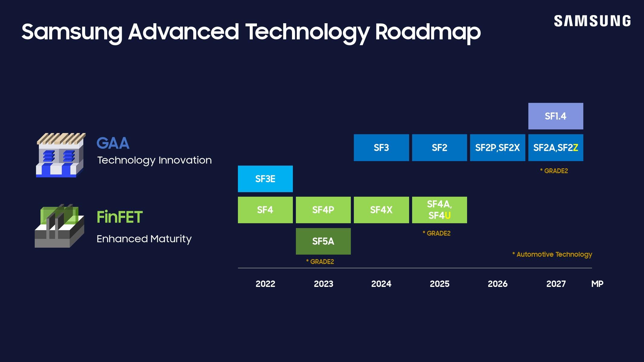 Credit: Samsung Foundry Shifting left HDL validation; security sign-off; a new eFPGA compiler; Rapidus-IBM packaging collaborationJune 11th, 2024 by Roberto Frazzoli
Let’s start with just a quick mention of a remarkable event in the IT world: at its recent Worldwide Developers Conference, Apple unveiled its long-awaited artificial intelligence strategy. Details of the AI innovations introduced by Apple – with a special focus on users’ privacy – can be found here. The Cupertino announcements, however, failed to impress the financial community, and Apple shares reportedly closed down nearly 2% after the event. Let’s now move to this week’s news roundup, which includes some pre-announcements concerning products that will be on display at the upcoming Design Automation Conference. Sigasi’s shift-left approach to HDL validation Sigasi has announced its new Visual HDL (SVH) product line, an integrated development environment that – according to the company – is able to take advantage of the shift-left methodology and give hardware designers and verification engineers better insight during the design progress. SVH enables them to manage HDL specifications by validating code early in the design flow, well before simulation and synthesis flows. SVH is fully integrated with Microsoft’s Visual Studio Code; lets users move through hierarchy views and graphics that update instantaneously as they make changes in their code; and flags problems while users enter HDL code. Starting with syntax and semantics, SVH enforces coding styles as recommended by safety standards such as DO-254 or ISO 26262 and catches UVM abuses. The new IDE comprises a tiered portfolio, offering a Designer Edition, a Professional Edition, an Enterprise Edition, and a Community Edition for non-commercial uses. Real Intent’s tool for RTL security sign-off Real Intent has announced Sentry, a hardware security static sign-off tool to protect designs against potential security vulnerabilities. The tool allows designers and security architects to incorporate hardware security sign-off early, as part of the RTL design process. According to the company, Sentry enables early hardware security sign-off at scale – supporting a hundred million gates with fast runtimes. Sentry analyzes data movement within the hardware, ensuring all paths adhere to stringent security protocols. In a single run, the tool performs path verifications simultaneously across multiple security specifications, such as data integrity (verifying that secure data transfers between protected domains without any corruption or unauthorized access), leakage prevention (ensuring sensitive data cannot reach unauthorized domains where it could be compromised) an interference safeguarding (stopping unauthorized data from reaching and interfering with secure domains). New chiplet description standard; AMD’s AI acceleration roadmap; Ultra Accelerator Link; 3-layer CMOS image sensorsJune 4th, 2024 by Roberto Frazzoli
Some of this weeks’ news updates are coming from Computex, Taiwan’s computer expo, which this year offered speeches from a lineup of semiconductor CEOs including AMD’s Lisa Su, Nvidia’s Jensen Huang, Intel’s Pat Gelsinger, Arm’s Rene Haas, and Qualcomm’s Cristiano Amon. While Computex isn’t the only thriving show in the IT world – just think of CES or MWC – it’s interesting to notice that its American and European counterparts died years ago. Las Vegas’ Comdex was held only until 2003; Hanover’s CeBit survived until 2018. Ansys simplifies cloud-based simulation on Azure Ansys has launched “Ansys Access on Microsoft Azure” to enable seamless deployment of pre-configured Ansys products on Azure cloud platform infrastructure. According to the company, Ansys’ customers using their own Azure subscription with existing Ansys licenses can now benefit from a more scalable, secure, and cost-effective approach to running HPC simulations in the cloud. As Ansys explained in a press release, there are many challenges that need to be addressed when using simulation in the cloud. These include validating on-premises workloads that have been shifted to the cloud, the ongoing work to deploy and test new virtual machines and configuring adjacent cloud-based infrastructure in a cost-effective manner. “Ansys Access on Azure” addresses these challenges by delivering pre-tested and configured Ansys applications updated with each major release and aligned to a curated set of recommended VMs and HPC infrastructure. According to Ansys, this simplifies implementation for IT departments, giving them better control over cost. IP quality assurance; PyTorch-to-RTL; Risc-V growth; new semi subsidies in China; Google’s human brain mappingMay 28th, 2024 by Roberto Frazzoli
Governments around the world keep subsidizing their respective domestic semiconductor industries, with the most recent announcements coming from China and South Korea. Meanwhile, artificial intelligence is accelerating human brain research, with Google spearheading this effort. But first, a few EDA-related updates. Siemens’ IP quality assurance solution Siemens Digital Industries Software has introduced Solido IP Validation Suite software, an automated signoff solution for quality assurance across all design intellectual property types, including standard cells, memories and IP blocks. The suite – which includes Siemens’ Solido Crosscheck software and Solido IPdelta software – aims to shorten the time-consuming task of validating IP across all its design views such as logical, physical, electrical, timing, and power analysis contexts. It also provides version-to-version IP qualification for more predictable full-chip IP integration cycles and faster time-to-market. Siemens’ PyTorch-to-RTL solution for AI accelerator design Siemens Digital Industries Software has announced Catapult AI NN software for High-Level Synthesis of neural network accelerators on ASICs and SoCs. Catapult AI NN starts with a neural network description from an AI framework such as TensorFlow, PyTorch or Keras, converts it into C++ and synthesizes it into an RTL accelerator in Verilog or VHDL for implementation in silicon. Catapult AI NN brings together hls4ml, an open-source package for machine learning hardware acceleration, and Siemens’ Catapult HLS software for High-Level Synthesis. Developed in close collaboration with Fermilab, a U.S. Department of Energy Laboratory, and other leading contributors to hls4ml, Catapult AI NN enables AI experts to develop PPA-optimized accelerators for different applications without requiring them to become ASIC designers. Innovations from the 2024 TSMC Technology SymposiumMay 20th, 2024 by Roberto Frazzoli
The European edition of TSMC’s 2024 Technology Symposium – held in Amsterdam on May 14 – allowed EDACafe to gain some additional insights on the innovations that the Taiwan-headquartered foundry first announced on April 24 at the North America edition of the event. Besides providing a roadmap of new opportunities for chipamkers and OEMs, these innovations also shed some light on the strategies that TSMC is planning to pursue over the next few years to retain its world-leading role. 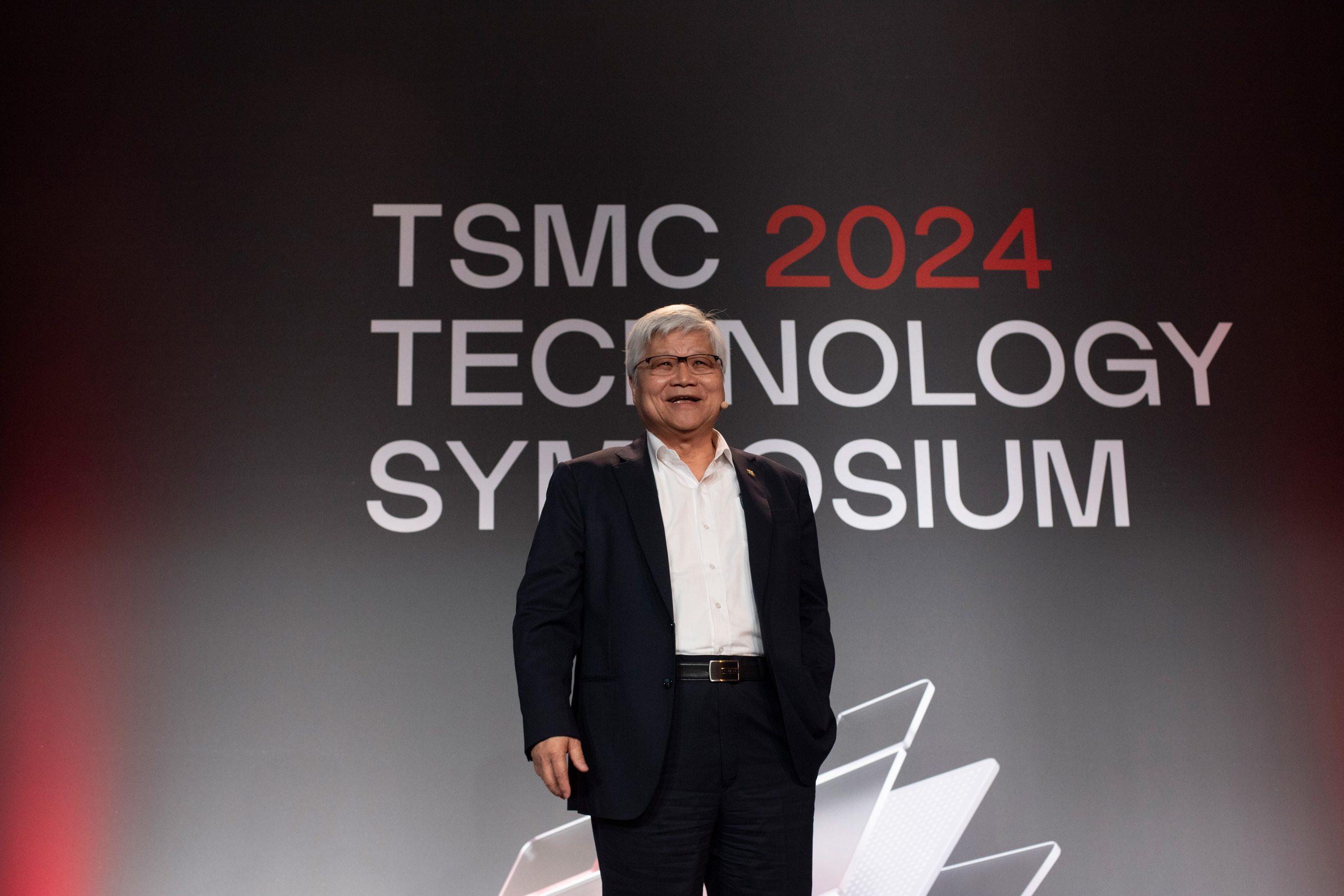 TSMC’s CEO C.C. Wei on stage in Amsterdam. Credit: TSMC Entering “the Angstrom era” with the A16 process Among TSMC’s most notable announcements is the upcoming nanosheet-based A16 process, where A clearly stands for Angstrom. Always keeping in mind what IEEE says about process names (i.e. that today they are just marketing labels, with no connection to the real size of transistor features), it’s inevitable to compare TSMC’s A16 process with Intel’s 18A process, and the difference in numbers – 16 vs 18 – suggests that the Taiwanese foundry hopes to leapfrog competitors even in the Angstrom era. According to the figures released by TSMC, the new A16 process – in comparison to the company’s N2P – will provide 8-10% speed improvement at the same Vdd (positive power supply voltage), 15-20% power reduction at the same speed, and up to 1.10X chip density improvement for data center products. The impact of these achievements can be significant considering large datacenters, where a 20% power reduction translates into a big amount of energy in absolute terms. TSMC’s A16 process is best suited for HPC products and is planned to enter production in 2026. As for moving existing designs to the new process, 86% of standard cells can be ported directly from N2P to A16, whereas 16% need a re-optimization. 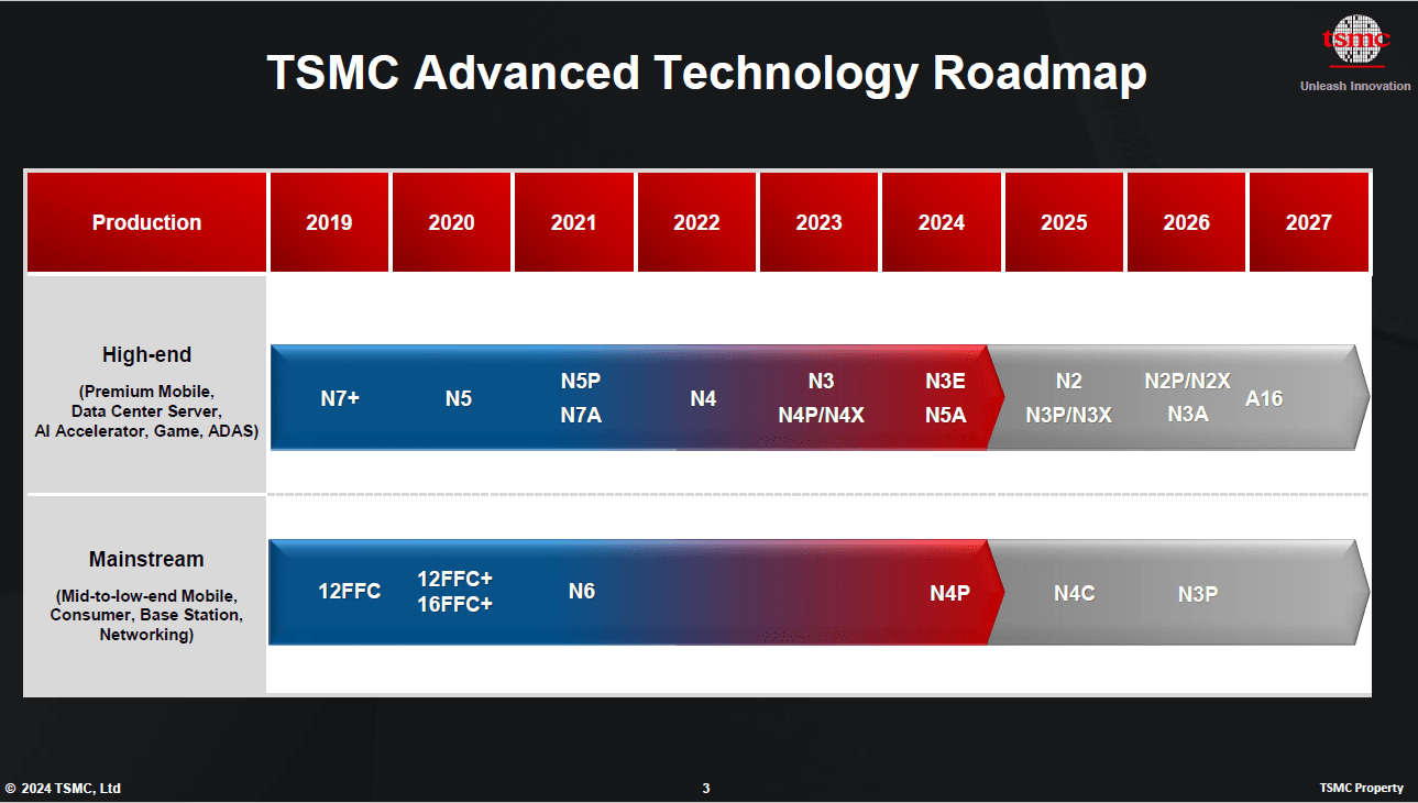 Credit: TSMC Read the rest of Innovations from the 2024 TSMC Technology Symposium Synopsys to sell Software Integrity Group; Micron to get CHIPS Act funding; 3D solution for RFSOI; recyclable PCBsMay 9th, 2024 by Roberto Frazzoli
An interesting side effect of the so-called “chip war” is that, now, even large news agencies are sometimes delving quite deep into technology topics. News agency Reuters has recently assigned reverse engineering experts to tear down a Huawei phone, to find out who made the chips inside it. The two companies that performed the analysis – iFixit and TechSearch International – found that Huawei’s Pura 70 Pro contains more China-made parts than previous models, highlighting the progress China is making towards technology self-sufficiency. Chinese components found in the high-end phone include a NAND memory that was likely packaged by Huawei’s in-house chip unit HiSilicon, and a Kirin 9010 processor that is likely a slightly improved version of the chip used by Huawei’s Mate 60 series. Synopsys to sell its Software Integrity Group After its recent Ansys acquisition, Synopsys is now focusing on EDA by selling its non-EDA division. The company has entered into a definitive agreement with Clearlake Capital Group and Francisco Partners, two global private equity firms, for the sale of its Software Integrity Group business in a transaction with a total value of up to $2.1 billion. Upon completion of the transaction, the business will emerge as a newly independent application security testing software provider. The existing Software Integrity Group management team is expected to lead the new privately held company, whose name has not been announced yet. Micron to get $6.1 billion CHIPS Act funding Micron Technology and the Biden-Harris Administration have signed a non-binding Preliminary Memorandum of Terms (PMT) for $6.1 billion in funding under the U.S. CHIPS and Science Act to support planned leading-edge memory manufacturing in Idaho and New York. Construction of the new Boise fab – which will be co-located with Micron’s R&D center – started in October 2023. The Idaho fab is expected to come online and be operational in 2025, with DRAM output starting in 2026. In New York, preliminary design, field studies and permitting applications are underway for the project; construction is expected to begin in 2025, with output starting in 2028. Samsung to receive CHIPS Act funding; AnsysGPT; new Palladium and Protium systems; Cadence’s cloud updatesApril 25th, 2024 by Roberto Frazzoli
EDA-related updates make up most part of this week’s news roundup, with Cadence in particular introducing several new products. But first, a CHIPS Act update. Samsung to get $6.4 billion under the US CHIPS and Science Act The U.S. Department of Commerce and Samsung Electronics have signed a non-binding preliminary memorandum of terms to provide up to $6.4 billion in direct funding under the CHIPS and Science Act. Samsung is expected to invest more than $40 billion in the US in the coming years. The proposed investment would turn Samsung’s existing presence in Texas into a comprehensive ecosystem for the development and production of leading-edge chips, including two new leading-edge logic fabs, an R&D fab, and an advanced packaging facility in Taylor, as well as an expansion to their existing Austin facility. Ansys’ AI-based virtual assistant Ansys has released its AI-powered virtual assistant, AnsysGPT, built using ChatGPT technology. The virtual assistant provides responses to queries concerning Ansys products, relevant physics, and other complex engineering topics – including simulation setup. AnsysGPT captures knowledge from new public sources, including product documentation, product and engineering-related training documentation, FAQs, technical marketing materials, and public Ansys Learning Forum discussions. Cadence’s new Palladium and Protium systems Cadence has announced the new Palladium Z3 Emulation and Protium X3 FPGA Prototyping systems, offering more than a 2X increase in capacity and a 1.5X performance increase compared to previous-generation systems. The Palladium Z3 and Protium X3 systems scale from job sizes of 16 million gates up to 48 billion gates, so the largest SoCs can be tested as a whole rather than just partial models. The new systems are powered by the Nvidia BlueField DPU and Nvidia Quantum InfiniBand networking platforms. Congruency is maintained when transitioning between the two systems and transitioning from virtual to physical interfaces and vice versa. The Palladium Z3 system accelerates hardware verification, and through functional and interface congruency, models can be quickly brought up onto the Protium X3 system for accelerated software validation. |
|
|
|||||
|
|
|||||
|
|||||


 Animation, 3D Art and 3D Models")