


EDACafe Editorial Roberto Frazzoli
Roberto Frazzoli is a contributing editor to EDACafe. His interests as a technology journalist focus on the semiconductor ecosystem in all its aspects. Roberto started covering electronics in 1987. His weekly contribution to EDACafe started in early 2019. AI agents in EDA; new AMD MI325X AI accelerator; low-power alternative to FP multiplication; China’s mature node productionOctober 15th, 2024 by Roberto Frazzoli
Let’s start by paying tribute to SpaceX’s engineering prowess: those who missed the incredible images of the Super Heavy booster rocket getting back on the launch pad – and then getting caught up by the launch tower – might want to catch up by watching this video from Bloomberg. ChipAgents: adding AI agents to existing EDA flows California-based startup Alpha Design has introduced ChipAgents, an artificial intelligence solution (an “AI agent”) meant to be added to existing EDA flows. According to the company, ChipAgents enables designers to transform their concepts into precise design specifications using simple language prompts; analyzes and generates RTL design specs and code; auto-completes Verilog; automates the creation of testbenches; and, through real-time learning from simulations, it autonomously verifies and debugs design code. New AMD Instinct MI325X accelerator challenging Nvidia H200 On occasion of its “Advancing AI” 2024 event, AMD announced its latest accelerator and networking solutions: the Instinct MI325X accelerators, the Pensando Pollara 400 NIC and the Pensando Salina DPU. According to the company, the Instinct MI325X accelerators deliver industry-leading memory capacity and bandwidth, with 256GB of HBM3E supporting 6.0TB/s, offering 1.8X more capacity and 1.3x more bandwidth than the Nvidia H200. The AMD Instinct MI325X also offers 1.3X greater peak theoretical FP16 and FP8 compute performance compared to Nvidia H200. This translates into up to 1.3X the inference performance on Mistral 7B at FP16, 1.2X the inference performance on Llama 3.1 70B at FP8 and 1.4X the inference performance on Mixtral 8x7B at FP16 of the H200. Besides introducing new chips, AMD has also confirmed it continues to invest in its ROCm open software stack for AI. New materials; Cerebras to go public; Amkor-TSMC collaboration; advancements in optical communicationOctober 7th, 2024 by Roberto Frazzoli
Artificial intelligence is the underlying theme for many of this week’s news updates, ranging from the development of new semiconductor materials to PCB assembly pricing. U.S. government-funded R&D on new materials: UWBGS, AI-powered experimentation Raytheon has been awarded a three-year, two-phase contract from DARPA to develop foundational ultra-wide bandgap semiconductors, or UWBGS, based on diamond and aluminum nitride technology. Phase one of the contract will focus on developing diamond and aluminum nitride semiconductor films and integrating them onto electronic devices. Phase two will focus on optimizing and maturing the use of these films onto larger diameter wafers for sensor applications. UWBGS defense applications will include radar and communication systems and high-speed weapon systems such as hypersonics. The U.S. Department of Commerce has announced an open competition demonstrating how AI can assist in developing new sustainable semiconductor materials and processes that meet industry needs and can be designed and adopted within five years. CHIPS for America anticipates up to $100 million in funding to award recipients that develop university-led, industry-informed, collaborations about artificial intelligence-powered autonomous experimentation (AI/AE) relevant to sustainable semiconductor manufacturing. AI/AE combines automated synthesis and characterization tools with an AI “planner” to determine the next round of an experimental campaign, vastly accelerating the design of new materials and the acquisition of materials data. Cerebras to go public Cerebras, the AI company mostly known for its wafer-scale chips, has filed a registration statement with the U.S. Securities and Exchange Commission relating to a proposed initial public offering of its Class A common stock. The company intends to list its stock on the Nasdaq Global Market under the ticker symbol “CBRS.” By reading the IPO paperwork, EETimes has found that a single customer, G42, accounted for 83% of Cerebras’ revenue in 2023 and 87% in the first half of 2024. G42 is an AI development holding company based in Abu Dhabi. TSMC-EDA updates; Google’s AI-based chip layout tool; new Altera FPGAs; double-faced GaN wafersSeptember 30th, 2024 by Roberto Frazzoli
Let’s start by briefly mentioning two U.S. CHIPS Act updates. Polar Semiconductor will receive up to $123 million in direct funding to expand and modernize the company’s manufacturing facility in Bloomington, Minnesota. The investment is expected to nearly double the U.S. production capacity of sensor and power chips. The U.S. government has also launched the National Semiconductor Technology Center’s (NSTC) Workforce Center of Excellence (WCoE), with an expected $250 million investment over ten years, to support education programs that address key skills and workforce gaps in the semiconductor industry. The first cohort of awardees consists of the following organizations: American Federation of Teachers Educational Foundation, Idaho Technology Council, Maricopa County Community College District, Rochester Institute of Technology, Texas A&M University, University of California Los Angeles, University of Illinois Urbana-Champaign. Latest EDA updates from TSMC OIP Forum North America On occasion of TSMC OIP Forum North America, held in Santa Clara on September 25, the major EDA vendors announced their latest tool certifications and new collaborations with the Taiwanese foundry. In general, tool certifications mainly concern TSMC’s N2 process, and areas of collaboration include backside power delivery for the foundry’s A16 process, 3D packaging, multiphysics simulation, IP, cloud-based EDA and more. Here are the announcements from Ansys, Cadence, Siemens and Synopsys. The agenda of the TSMC event, with abstracts of the presentations, can be found here. Below, two charts summarizing the news from Cadence and Synopsys. 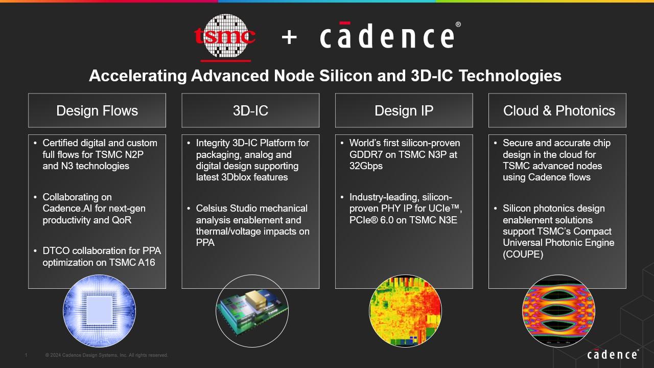 Credit: Cadence, TSMC 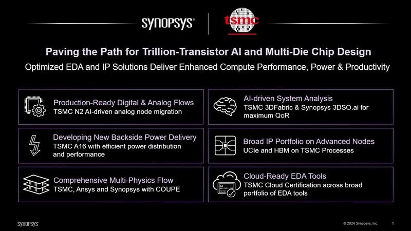 Credit: Synopsys, TSMC Rumored Qualcomm-Intel deal; Synopsys selling optical group to Keysight; new NAND chipsSeptember 23rd, 2024 by Roberto Frazzoli
Troubled Intel continues to be in the spotlight, also for the rumors of a gigantic acquisition that analysts deem unlikely. EDA news this week include Synopsys continuing to adjust its market footprint as a consequence of the Ansys acquisition. NAND chips are in the news not just because of new product announcements, but also as a benchmark of China’s manufacturing capabilities in the so-called “chip war” era. Intel’s CEO message In a message to Intel employees, company CEO Pat Gelsinger emphasized two recent good news: Intel Foundry will produce an AI fabric chip for AWS using the company’s 18A process – as part of a broader partnership – and Intel as a whole has been awarded up to $3B in direct funding under the CHIPS and Science Act for the U.S. government’s Secure Enclave program, designed to expand the trusted manufacturing of leading-edge semiconductors for the U.S. government. Gelsinger also announced that the company plans to establish Intel Foundry as an independent subsidiary inside of Intel, completing the process initiated earlier this year when the company separated the P&L and financial reporting for Intel Foundry and Intel Products. As for the new fabs, Gelsinger said that the company will pause its projects in Poland and Germany by approximately two years based on anticipated market demand. According to Reuters, Qualcomm has in recent days approached Intel to explore a potential acquisition of the troubled chipmaker. Qualcomm CEO Cristiano Amon would be personally involved in the negotiations, however the San Diego-based company has not made a formal offer for Intel. The Reuters report points out that it’s not clear how Qualcomm, which has a market value of $188 billion, would finance a bid for Intel, which is valued at $122 billion, including its debt, and how it would handle the takeover of Intel Foundry. 40 Gbps UCIe IP; 300-mm GaN wafers; new edge AI SoCs; new US export controlsSeptember 12th, 2024 by Roberto Frazzoli
Just a quick update somewhat related to the Intel situation, before moving to this week’s news roundup. According to a Reuters report, Qualcomm has explored the possibility of acquiring portions of Intel’s design business. While being mostly interested in Intel’s client PC design business, Qualcomm would be looking at other design units as well. Synopsys’ 40 Gbps UCIe IP Synopsys has announced what it claims is the industry’s first complete UCIe IP solution operating at up to 40 Gbps per pin, supporting both organic substrate and high-density, advanced packaging technologies. Capabilities of the new Synopsys 40G UCIe IP solution include single reference clock; die-to-die link initialization without the need to load the firmware; test and silicon lifecycle management features; support for AXI, CHI chip-to-chip, streaming, PCI Express, and CXL; a pre-verified design reference flow. Synopsys’ Imaging System Simulator Synopsys has also announced ImSym (Imaging System Simulator), a virtual prototyping platform for imaging systems, encompassing lenses, sensors, and image signal processors into a comprehensive end-to-end simulation platform. Powered by CODE V and LightTools optical design software, ImSym offers a quantitative end-to-end simulation flow, thus reducing the need for physical prototypes. Read the rest of 40 Gbps UCIe IP; 300-mm GaN wafers; new edge AI SoCs; new US export controls Intel’s troubles; GF’s new partnerships; PSS 3.0; new Risc-V startup; future of DRAMSeptember 5th, 2024 by Roberto Frazzoli
After many joys, the stock exchange gave some sorrows to Nvidia on September 3 when the company’ shares reportedly lost 9.5% in what is considered “the deepest ever single-day decline in market value for a U.S. company”. In absolute terms, Nvidia lost $279 billion in market capitalization, an indication – according to some observers – that investors are becoming more cautious about AI technology. Intel reportedly considering selling Altera Intel’s troubles inevitably are in the spotlight this week. Let’s quickly recap some of the latest updates, based on Reuters reports. Intel CEO Pat Gelsinger and key executives are expected to present a plan in mid-September to cut unnecessary businesses and revamp capital spending. This plan could include selling Altera – but not Intel Foundry – and pausing or halting the new fab in Magdeburg, Germany. Analysts and investors think Intel will likely be removed from the Dow Jones Industrial Average index, due to the stock’s near 60% decline this year. A Republican senator has asked Gelsinger for more details on Intel’s plans to cut more than 15,000 jobs despite being set to receive nearly $20 billion from the U.S. CHIPS Act. Former Cadence CEO Lip-Bu Tan left the Intel board – where he was sitting – as he grew “frustrated by Intel’s large workforce, its approach to contract manufacturing and its risk-averse and bureaucratic culture.” GlobalFoundry’s new partnerships And Lip-Bu Tan gave a keynote address at this year’s GlobalFoundry Technology Summit in Santa Clara. The event was the occasion for announcing GF’s partnerships with Efficient and Finwave. US-based startup Efficient will use GF’s 22FDX process to build its ultra-low-power CPUs. The implementation will also take advantage of 22FDX’s MRAM and Adaptive Body Biasing (ABB) capabilities. According to Efficient, current general-purpose processors are over-designed for generality, with most of their energy consumed by unnecessary internal data movement and instruction control overheads. The Efficient Fabric processor architecture, instead, is based on a dataflow execution model and provides reconfigurable hardware at compile time – promising up to 99% lower DC power without compromising performance. Massachusetts-based Finwave will collaborate with GF to optimize and scale its RF GaN-on-Si enhancement-mode (E-mode) MISHEMT technology to volume production at GF’s 200mm fab in Burlington, Vermont, using the foundry’s 90RFGaN platform. Target applications include power amplifiers in future mobile phones. New AI inference solutions; a new Risc-V IP player; Chips Act updates; low power EUV litho; MEMS-based air coolingAugust 28th, 2024 by Roberto Frazzoli
Catching up on some of the August news after the summer break, let’s start by briefly recalling Intel’s disappointing second-quarter results and the company’s cost-reduction plan: Intel will cut its headcount by more than 15%, with the majority completed by the end of 2024. Consistently with the cost-reduction plan, Intel has reportedly sold its share stake in Arm. More news this week include new solutions challenging Nvidia AI dominance, just when Nvidia’s Blackwell family is experiencing issues in reaching high volume production. According to SemiAnalysis, the problems are related to the complexity of TSMC’s CoWoS-L packaging technology and insufficient capacity for this specific version of the package. TSMC’s European joint venture holds groundbreaking ceremony On August 20, ESMC – a joint venture between TSMC, Bosch, Infineon and NXP – held a groundbreaking ceremony for its first semiconductor fab in Dresden, Germany. When fully operational, ESMC is expected to have a monthly production capacity of 40,000 300mm wafers on TSMC’s 28/22 nanometer planar CMOS and 16/12 nanometer FinFET process technology. Total investments are expected to exceed 10 billion euros consisting of equity injection, debt borrowing, and strong support from the European Union and German government. Fraunhofer’s Chiplet Center of Excellence Also based in Dresden, Germany, is the Chiplet Center of Excellence (CCoE) launched by three Fraunhofer Institutes with the purpose of partnering with industry to drive forward the introduction of chiplet technology. The CCoE will initially focus on automotive applications, developing the first workflows and methods for electronics design, demonstrator construction, and the evaluation of reliability. The Fraunhofer initiative adds to the already existing “Automotive chiplet program” from Belgian technology hub imec. Amkor to get CHIPS Act funds; startup funding; Synopsys acquires Valtrix; liquid cooling growthAugust 1st, 2024 by Roberto Frazzoli
Scarce supply isn’t the only issue worrying hyperscalers when it comes to relying on Nvidia GPUs: the other factor is high price. The quest for a cheaper, homegrown alternative is driving Amazon’s chip development effort, according to a Reuters report. And Nvidia’s dominant position in the AI market prompted U.S. progressive groups and Democratic Senator Elizabeth Warren to press the Department of Justice to investigate the GPU leader over competition concerns. Meanwhile, Cerebras – an Nvidia competitor – has reportedly filed for an initial public offering in the United States, in a confidential manner. Ultra Librarian-Footprintku AI partnership Ultra Librarian has announced a partnership with Footprintku AI aimed at bringing Footprintku AI’s technologies in Design-for-Manufacturing (DFM) processes into the Ultra Librarian CAD library. Goal of this collaboration is to provide a new on-demand DFM-aware library for companies looking to enhance and validate their libraries for DFM. New fab updates: Amkor, SK hynix Packaging service provider Amkor has signed a non-binding preliminary memorandum of terms with the US Department of Commerce to receive proposed funding as part of the CHIPS and Science Act. Amkor announced in November 2023 its plans to build its first domestic OSAT (outsourced semiconductor assembly and test) facility in Peoria, Arizona. The company projects to invest approximately $2 billion and employ approximately 2,000 people at the new facility. Upon completion, this will be the largest outsourced advanced packaging and test facility in the United States. The terms include up to $400 million in proposed direct funding, and access to $200 million in proposed loans. EDA updates; new AI approaches; hi-res thermal mapping; dumb LLMsJuly 25th, 2024 by Roberto Frazzoli
Memory-based neural networks and the use of “sparse AI” at the edge are two new AI approaches included in this week’s news roundup. Reasoning failures from LLMs are discussed in our Further Reading section. But first, some EDA updates. EDA updates: DeFacto, Ansys, Keysight, Synopsys DeFacto and Arm have developed a joint design flow for Arm-based SoCs, covering the steps from SoC design architecture and exploration down to the generation of RTL and IP-XACT design files. The flow integrates Arm IP Explorer and Defacto SoC Compiler. The generated files are fully compatible with standard RTL2GDS SoC design flows. According to DeFacto, the joint solution significantly reduces the overall design time from specification to an SoC ready for synthesis. Ansys is collaborating with Supermicro and Nvidia to deliver turnkey hardware, enabling acceleration for Ansys multiphysics simulation solutions. According to Ansys, sizing and configuring the right hardware for multiphysics simulation is a complex task that can significantly impact performance, cost, and productivity. Turnkey, customized hardware solutions with CPUs, GPUs, interconnects, and cooling modules allow engineers to run predictively accurate simulations more efficiently. The testing process revealed accelerations ranging from 4x to 1,600x, for different Ansys tools. Read the rest of EDA updates; new AI approaches; hi-res thermal mapping; dumb LLMs New US GlobalWafers fabs; new AI robotic model; SoftBank acquires Graphcore; semiconductor-specialized LLMJuly 18th, 2024 by Roberto Frazzoli
Not surprisingly, several interesting updates this week regard artificial intelligence in one way or another. Among them, the news about robotic startup Skild attracts the attention on the marriage between AI and robotics, a promising perspective also from the point of view of the study of living beings. So far, AI has achieved incredible language-centric performance: AI can even emulate the skills of a semiconductor expert, just see the news about SemiKong below. But throughout evolution, language is just the latest addition to a range of other key functions that are still difficult if not impossible to artificially replicate. Motion control is definitely one of those key functions: still today, we have no idea of how we could build a robot performing like a playing kitten – a small mammal, very far away from human beings in the evolution tree. In nature, there is no such thing as a language skill without a body, and there has to be a reason for that. So focusing on motion control sounds like approaching the problem from the right side. GlobalWafers to get CHIPS act funding The U.S. Department of Commerce plans to provide up to $400 million under the CHIPS and Science Act to Taiwan-headquartered GlobalWafers to build and expand facilities in Sherman, Texas (to establish the first 300mm silicon wafer manufacturing facility for advanced chips in the United States) and in St. Peters, Missouri (to establish a new facility to produce 300mm silicon-on-insulator wafers). Further, GlobalWafers plans to convert a portion of its existing silicon epitaxy wafer manufacturing facility in Sherman, Texas to silicon carbide epitaxy wafer manufacturing, producing 150mm and 200mm SiC epitaxy wafers. |
|
|
|||||
|
|
|||||
|
|||||


 Animation, 3D Art and 3D Models")