


EDACafe Editorial Roberto Frazzoli
Roberto Frazzoli is a contributing editor to EDACafe. His interests as a technology journalist focus on the semiconductor ecosystem in all its aspects. Roberto started covering electronics in 1987. His weekly contribution to EDACafe started in early 2019. Geopolitical tensions; fab updates; reverse engineering surprises; interconnect updates; acquisitionsAugust 5th, 2022 by Roberto Frazzoli
Catching up on some of the news from the last thirty days or so, several updates obviously concern U.S.-China tensions. As far as the semiconductor industry is concerned, news includes additional export restriction being considered by the U.S Government to halt China’s advances in semiconductor manufacturing, but the intricacies of a globalized ecosystem may cause side effects. According to analysts quoted by Reuters, export restrictions could also impact China-based memory fabs belonging to South Korean manufacturers such as Samsung and SK Hynix. A similar impact could be caused by export restrictions on European semiconductor equipment: for example – according to Reuters – the export ban has prevented SK Hynix from installing ASML’s EUV lithography equipment in its DRAM fab in Wuxi, China. Meanwhile, China’s IC sales keep increasing: according to market analysis firm TrendForce, the growth rate was 17% in 2020, 18.2% in 2021 and it is expected to be 11.21% in 2022. Fab and foundry updates: SkyWater, Micron, ST-GlobalFoundries, IFS-MediaTek, Intel-TSMC Also related to geopolitical tensions is the recent passing of the U.S. ‘Chips and Science Act’. Some companies have already announced their intentions to leverage this public funding measure: among them, U.S. foundry SkyWater plans to build a $1.8 billion semiconductor R&D and production facility in Indiana through a public-private partnership with the State and Purdue University; and U.S. memory maker Micron Technology intends to invest “in bringing the most innovative leading-edge memory manufacturing to the U.S.” More details regarding Micron’s plans are expected in the coming weeks. SaaS-based system design and analysis goes e-commerce with Cadence OnCloudJuly 29th, 2022 by Roberto Frazzoli
OrCAD and Allegro PCB design technologies, Clarity/Sigrity/Celsius system analysis technologies, and Fidelity CFD software are now available from a SaaS platform, through a consumption-based pricing model Ease of purchase is undoubtedly one of the reasons for success of many consumer-oriented services provided through the Internet: just type a card number, freely select a quantity or a subscription duration, and you immediately get what you want. With EDA technologies now available through cloud computing platforms, this ease of purchase can also be extended to the use of EDA tools – adding to the main benefit of a Software-as-a-Service model: eliminating the need for expensive infrastructure hardware. These, in short, are the concepts behind OnCloud, the new Cadence e-commerce platform for cloud-based system design and analysis. With OnCloud, the ease of purchase enabled by e-commerce is leveraged to address two types of customer needs: on the one hand, making it easier for the ‘long tail’ of small EDA users to access first-class technologies; on the other hand, enabling big EDA users to cope with workload peaks without purchasing additional licenses. Two Cadence executives – Ben Gu, Vice President of R&D for the Multiphysics System Analysis Business Unit, and Mahesh Turaga, Vice President of Business Development, Cloud – described the OnCloud features in the video interview they recently gave to EDACafe’s Sanjay Gangal; in this article we will add a few details, as well as the answers Turaga provided to some additional questions.
Read the rest of SaaS-based system design and analysis goes e-commerce with Cadence OnCloud Turnkey ASIC outsourcing – Presto Engineering’s proposal to Original Device ManufacturersJuly 22nd, 2022 by Roberto Frazzoli
According to the European company specializing in semiconductor design and services, it is now possible to bring an ASIC to market for less than $5 million dollars in upfront investment – and customers lacking semiconductor expertise can lower the risks by outsourcing to Presto the entire ASIC procurement process, from design to delivery It’s a two-speed world: on the one hand, applications such as smartphones or artificial intelligence accelerators keep pushing the semiconductor industry towards Angstrom-scale process nodes and hundreds of billions transistor counts; on the other hand, many end products in a variety of markets – from industrial to medical and more – are still relying on an electronic box containing a PCB with a number of low-integration ICs and discrete components. Replacing the old-style box with an ASIC would clearly provide multiple benefits to the end product, but manufacturers lacking a semiconductor expertise are concerned by the risks of a complex production process. Targeting this largely untapped market, a France-headquartered company called Presto Engineering is addressing European and American manufacturers with a two-pronged message: ASICs are now cheaper and easier to make than ever before, and risks can be reduced by outsourcing the entire ASIC procurement process – from design to delivery – to Presto. Michel Villemain, CEO of Presto Engineering, described his company’s offering in the video interview he recently gave to EDACafe’s Sanjay Gangal; in this article we will add a few details, as well as the answers he provided to some additional questions.
AI-driven system design optimization with Cadence Optimality ExplorerJuly 15th, 2022 by Roberto Frazzoli
From a chip to another, traveling through a package, a printed circuit board, and another package: the trip of a high-speed electric signal inside a system is fraught with perils. And avoiding that signals arrive weak and ‘dirty’ at their final destinations is just one of the system-level challenges facing designers today: with ever higher package densities, finer PCB traces, and higher frequencies, crucial aspects now include cooling, stress and more. At the system level, therefore, the interactions among electrical, mechanical, electromagnetic and thermal aspects can no longer be neglected. Unfortunately, the combination of so many different parameters generates an immensely large design space, that system designers are supposed to thoroughly explore to find the optimal solution.
Besides being very human-intensive and requiring a lot of time and computing resources, this task is often hindered by organizational ‘silos’ preventing collaboration among experts from different disciplines. Now a new solution from Cadence, called Optimality Explorer, promises a ten times faster system design optimization – with up to a 100X speedup on some designs – by applying artificial intelligence to a “Multi-disciplinary analysis and optimization” (MDAO) approach. Ben Gu, vice president of R&D for the Multiphysics System Analysis Business Unit at Cadence, described Optimality in the video interview he recently gave to EDACafe’s Sanjay Gangal; in this article we will add a few details, as well as the answers he provided to some additional questions. A quick look at the DAC 2022 conference programJuly 8th, 2022 by Roberto Frazzoli
The Design Automation Conference is back to its usual summer timeframe – again at the Moscone Center in San Francisco – with over one hundred exhibitors and a rich conference program that covers a wide range of topics including artificial intelligence, autonomous systems, Risc-V, security, embedded systems and more. Here we will briefly highlight some of the conference content more directly related to EDA, referring readers to the conference program for the detailed schedule. EDA vendors’ top executives on stage: keynotes and panels As usual, the DAC will offer attendees the opportunity to listen to EDA vendors’ top executives and – to some extent – to ask them questions. This year’s keynoters will include Anirudh Devgan, Cadence CEO, speaking about “Computational Software and the Future of Intelligent Electronic System Design”. More EDA executives will give speeches as part of a series called SKYTalks: Joe Sawicki from Siemens EDA (“Delivering ‘Smarter’ Faster: The Future of EDA & AI”), and Sandeep Mehndiratta from Synopsys (“It’s Getting Cloudy Out There”). Among the panels featuring EDA vendor executives, the top spot obviously goes to John Cooley’s DAC Troublemaker Panel, offering attendees the opportunity to hear “edgy questions” being asked to Joe Sawicki (Siemens EDA), Tom Beckley (Cadence), Dean Drako (IC Manage), Prakash Narain (Real Intent), Tony Chan Carusone (Alphawave IP) and Sam Appleton (Ausdia).
Samsung’s 3-nm GAA in production; training large NLP models on a single Cerebras device; reducing metal line resistanceJuly 1st, 2022 by Roberto Frazzoli
Quick updates on the impact of Ukraine war. Global exports of semiconductors to Russia have reportedly slumped by 90% due to export controls. And U.S. Commerce Secretary Gina Raimondo has reportedly threatened to “shut down” China’s SMIC foundry if it is found to be supplying chips to Russia. “We will shut them down and we can, because almost every chip in the world and in China is made using U.S. equipment and software,” she said. Moving to new fab updates, Taiwan’s GlobalWafers will reportedly invest $5 billion on a new plant in Sherman, Texas, to make 300-millimeter silicon wafers, switching to the United States after a failed investment on Germany’s Siltronic. Samsung’s 3-nm GAA in production Samsung Electronics has announced that it has started initial production of its 3-nanometer process node applying its Gate-All-Around (GAA) transistor architecture called Multi-Bridge-Channel FET (MBCFET), enabling a supply voltage reduction and a higher drive current capability. Initial applications are targeting high performance, low power computing, with plans to expand to mobile processors. According to the company, Samsung’s proprietary technology – which utilizes nanosheets with wider channels – allows higher performance and greater energy efficiency compared to GAA technologies using nanowires with narrower channels. However, channel width in Samsung’s 3nm GAA technology can be adjusted to obtain various power/performance combinations. Compared to 5nm process, Samsung claims that the first-generation 3nm process can reduce power consumption by up to 45%, improve performance by 23% and reduce area by 16%; the second-generation 3nm process is expected to reduce power consumption by up to 50%, improve performance by 30% and reduce area by 35%. 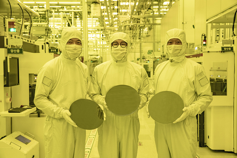 Photo: Business Wire New fab rumors; TSMC’s innovations; low-temperature 3D chip bonding; new optical microphoneJune 24th, 2022 by Roberto Frazzoli
The so-called metaverse now has its standardization initiative: called Metaverse Standards Forum, it brings together a few dozen founding members including Meta (Facebook), Microsoft and Nvidia – but, as noted by Reuters, the member list currently does not include Apple. However, “the Forum is open to any company, standards organization, or university at no charge,” says the announcement press release, so never say never. Let’s now move to our usual news round-up, that this week includes a couple of interesting academic works. Quick EDA updates Keysight’s PathWave RFPro, integrated with the Synopsys Custom Compiler design environment, is enabled to support TSMC’s newest N6RF Design Reference Flow. Pulsic has added new features to its Unity product. Among them, Unity Chip Planning technology now can handle incremental floorplans; and the embedded integrations with Cadence Virtuoso and Synopsys Custom Compiler allow users to access Unity directly from these systems. Cadence’s Design IP offering has already achieved over twenty design wins in TSMC’s 5nm process technology, with multiple first-pass silicon successes. Xpeedic has recently released its latest RF EDA/Filter Design Platform 2022. Backside power delivery; GaN-on-Si for 5G; Apple’s M2; new Fraunhofer centerJune 16th, 2022 by Roberto Frazzoli
Geopolitical issues keep making news: a team of U.S. investors, scientists, operators, and national security experts has founded America’s Frontier Fund (AFF), described as “the nation’s first non-profit strategic investment fund focused on building and scaling breakthrough deep-tech companies and platforms for the national interest.”. Led by CEO and co-founder Gilman Louie, AFF intends to counter “authoritarian nations” that “are committed to out-spending and out-innovating the U.S. to gain military and economic superiority.” The fund’s initial areas of focus will include microelectronics, artificial intelligence, new materials, quantum sciences, next generation networks (5G/6G), advanced manufacturing, and synthetic biology. Let’s now move to other news updates, this week with a significant presence of European research centers. Imec demonstrates backside power delivery with buried power rails Belgian research institute Imec has demonstrated a routing scheme for logic ICs with backside power delivery enabled through nano-through-silicon-vias (nTSVs) landing on buried power rails (BPRs). The BPRs connect to scaled FinFET devices whose performance was not impacted by backside wafer processing. The novel routing scheme with decoupled power and signal wiring acts as a scaling booster for future logic technologies (2nm and beyond), as the nTSVs land on BPRs with tight overlay control and are implemented at a tight pitch of 200nm without consuming any area of the standard cell. The solution also offers a system performance benefit by improving the power delivery, as it reduced IR voltage drop. Additionally, Imec demonstrated a performance boost by implementing a 2.5D MIMCAP (metal-insulator-metal capacitor) in the backside serving as a decoupling capacitor. Backside power delivery – using the back side of the wafer to route power lines, in order to alleviate routing congestion on the front side and reduce IR voltage drop – can be implemented in different ways; Imec believes that combining it with buried power rails is the most promising implementation scheme.  TEM image showing scaled FinFET devices connected to the wafer’s backside (through nTSVs and BPR) and frontside (through BPR, VBPR and MOA). Copyright: Imec Read the rest of Backside power delivery; GaN-on-Si for 5G; Apple’s M2; new Fraunhofer center AI/ML-based optimization; free GPU and DLA IPs; easier I3C adoptionJune 9th, 2022 by Roberto Frazzoli
According to Reuters reports on the impact of Ukraine war, more U.S. tech companies are leaving Russia: Microsoft is substantially cutting its activity in the country, while IBM is closing its Russian business and has started to lay off its employees. Russia, for its part, has limited exports of noble gases including neon – used in chip fabrication – until the end of 2022. Exports will be allowed only with special State permission. Let’s now move to our usual tech news round-up, starting with a brief update on TSMC’s roadmap: the Taiwanese foundry has reportedly chosen the nanosheet transistor architecture for its next 2-nanometer node starting in 2025. As for EDA, the use of artificial intelligence/machine learning in chip design is in the spotlight this week with two significant announcements. Synopsys’ machine learning-based design optimization solution Synopsys has introduced DesignDash, a design optimization solution based on machine learning and big data analytics. According to the company, DesignDash enhances design productivity in different ways: by providing real-time design status through visualizations and interactive dashboards; deploying deep analytics and machine learning to extract and reveal actionable understanding from vast volumes of structured and unstructured EDA metrics and tool-flow data; classifying design trends, identifying design limitations, providing guided root-cause analysis and delivering flow consumable, prescriptive resolutions. The solution complements the Synopsys SiliconDash product, part of the Synopsys Silicon Lifecycle Management Family. Read the rest of AI/ML-based optimization; free GPU and DLA IPs; easier I3C adoption War impact on EVs; China’s AI chips investments; Meta-Broadcom deal; ORNL’s exaflop computerJune 2nd, 2022 by Roberto Frazzoli
China is among the themes of this week’s roundup, with news concerning both its richly funded AI chip providers and – despite growing geopolitical tensions – its attractiveness for European investments. Merck to build a new site in China Germany-based Merck KGaA has reportedly signed a contract to open a base in the Chinese city of Zhangjiagang, describing it as its largest single electronics business investment in the country. In the new site, a 69-acre lot, Merck will build production facilities for thin film materials and electronic specialty gasses, along with a warehouse and operation centers. “China is currently the fastest growing semiconductor manufacturing market worldwide,” Merck China President Allan Gabor reportedly said in a statement. “We believe a golden era for China’s semiconductor industry has just begun,” he added. Will Ukraine war accelerate transition to electric vehicles? War in Ukraine is causing a shortage of wire harnesses – the complex and heavy cable bundles connecting all the electrical/electronics components of a vehicle – as the Eastern European country is a major supplier of these products. The shortage could accelerate transition from traditional vehicle network architectures based on “domain ECUs” to the new architectures based on “zonal ECUs”, which enable a dramatic simplification of vehicle wiring. This, at least, is the opinion of the industry experts quoted in a recent Reuters report. Simpler and lighter cable bundles would reduce carmakers dependence on Ukraine and other countries with a low labor cost, but their adoption would require redesigning the vehicles’ data and power networks. This could prompt a quicker phase-out of gasoline and diesel vehicles, as carmakers would rather not invest money in redesigning products that are approaching the end of their lives. Zonal ECUs are also paving the way to new wiring technologies such as the flexible circuits developed by CelLink (San Carlos, CA), already being used in ‘native’ electric cars. |
|
|
|||||
|
|
|||||
|
|||||


 Animation, 3D Art and 3D Models")