EDACafe Editorial Roberto Frazzoli
Roberto Frazzoli is a contributing editor to EDACafe. His interests as a technology journalist focus on the semiconductor ecosystem in all its aspects. Roberto started covering electronics in 1987. His weekly contribution to EDACafe started in early 2019. A quick look at some IEDM innovations; bioinspired neural networks; EDA updatesNovember 27th, 2023 by Roberto Frazzoli
Will artificial intelligence ever be able to replicate biological brains? It’s a fact that research is advancing on all fronts. On the one hand, the semiconductor industry continues to push transistor size reduction – examples can also be found in some of this year’s IEDM papers – paving the way to systems comprising an ever larger number of transistors. On the other hand, scientists have started bridging artificial intelligence and neurosciences to explore overall network structures – as in recent research from Cambridge University – extending the concept of “neuromorphic” beyond using spiking neurons. This week we will briefly touch these topics – but first, a couple of EDA-related updates. Cloud-based simulation of mechanical stress for TSMC’s 3D packaging Ansys has collaborated with TSMC and Microsoft to validate a joint solution for analyzing mechanical stresses in multi-die 3D-IC systems manufactured with TSMC’s 3DFabric advanced packaging technologies. The solution is based on Ansys Mechanical finite element analysis software running on Microsoft Azure cloud infrastructure. 3D-IC systems often have large temperature gradients that lead to intense mechanical stresses between components due to differential thermal expansion. These stresses can lead to cracking or shearing of the connections between various elements. Simulating thermomechanical stress for large and complex devices, while maintaining predictive accuracy, requires substantial computing power. New release of QuickLogic tool suite QuickLogic has released version 2.4 of its Aurora eFPGA development tool suite. According to the company, this newest version integrates core tool enhancements that improve the eFPGA utilization and performance of designer’s RTL, particularly in the area of reconfigurable computing. The tool suite integrates fully open-source modules for scalability, longevity, and full code transparency. New features include asymmetric BlockRAM (BRAM) inferencing to reduce the need for manual modification of a user’s RTL design; single stage routing algorithm that boosts maximum operating frequency of a design by up to 24%; power calculation; and other new functionalities.
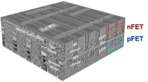
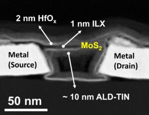
A quick look at some IEDM papers Let’s take a quick look at some of the highlights from the upcoming IEDM conference, which will be held in-person December 9-13, 2023 in San Francisco. One of the key topics will be the advancements towards complementary FETs (CFETs), 3D designs where n-FET and p-FET nanosheets are stacked on top of one other. CFETs are widely considered as the next step to continue shrinking transistors size. At IEMD, TSMC will describe a monolithic CFET architectural approach for logic technology scaling, featuring 48nm-gate-pitch stacked n-FET-on-p-FET silicon nanosheet transistors. The device demonstrated a six orders of magnitude on/off current ratio and a >90% yield. The gate pitches of the devices demonstrated by previous work were too large for future scaling, while this work achieved a 48nm gate pitch. This was obtained with a vertically stacked n/p source-drain epitaxy, comprising middle dielectric isolation, an inner spacer, and n/p SD isolation. Intel will discuss a 3D monolithic CFET device consisting of three n-FET nanoribbons on top of three p-FET nanoribbons, with 30nm of vertical separation between them. They used this device to build fully functional inverters at a 60nm gate pitch. The devices feature vertically stacked dual-S/D epitaxy; dual metal work function gate stacks connecting the n- and p- transistors; and integration with backside power delivery and direct backside device contacts. Another promising solution for further scaling is the use of transition metal dichalcogenides such as MoS2 (molybdenum disulfide, suitable for n-type devices) or WSe2 (tungsten diselenide, better suited for p-type devices), just one atomic layer thick, to replace silicon as the channel material. On this topic, TSMC-led teams will discuss unprecedented performance from two stacked NMOS nanosheets with MoS2 channels, and well-matched n- and p-MOS transistors with channels made using MoS2 and WSe2, respectively. In these devices, the p-FET mobility reached a record high level. As for memories, another TSMC-led team will describe an STT-MRAM (Spin-Transfer Torque magnetoresistive RAM) with a 1S1R (1 selector/1 resistor) crosspoint array architecture, having more than twice the density of conventional 1T1R (1 transistor/1 resistor) designs at a 16nm technology node. What makes this possible is the use of a specially engineered selector material, SiNGeCTe. The memory shows high-speed switching and outstanding read/write endurance (>1e9/>1e6 cycles, respectively). STT-MRAM is considered an alternative to flash memories at advanced nodes. Samsung researchers will discuss a way to scale DRAM further (sub-10nm) with vertical-channel transistors (VCTs) using IGZO (indium gallium zinc oxide) as the channel material. They integrated a 4F2 single-gated IGZO-VCT, monolithically stacked on top of core/peripheral transistors with no need for wafer bonding. The vertical architecture also can fully suppress ‘row hammer interference’, because the active region isn’t shared with adjacent cells. As for power devices, Intel will unveil the first integrated device combining a GaN channel with a CMOS driver, in 300mm GaN-on-Si technology. The researchers will detail a new gate-last process flow for the 3D monolithic integration of GaN and Si CMOS by layer transfer, where high-temperature activation steps for the Si CMOS transistors are completed before the gate dielectric of the GaN MOSHEMT is deposited. This resolves a major hurdle in the 3D monolithic integration of GaN and Si CMOS transistors. As for imaging, Samsung researchers will describe a stacked three-layer 64-megapixel CMOS image sensor (CIS) architecture with 0.5µm pixels, the smallest ever reported. A key feature of the device is that it uses copper-to-copper bonding to interconnect pixels from layer-to-layer, which aligns them precisely and thereby reduces the size of the CIS, and also reduces parasitic capacitance. Space constraints cause neural networks to develop brain-like features Researchers from Cambridge University have studied the features of what they have called “spatially-embedded recurrent neural network” (seRNN), that is, a network in which each neuron is characterized by its X, Y, and Z coordinates in space – so that it is possible to calculate the distance between any two neurons. Then they constrained the evolution of the network by incentivizing minimization of long distance connections, a biologically plausible requirement: “A brain network must overcome metabolic costs of growing and sustaining the network within its physical space, while simultaneously implementing its required information processing,” the researchers observed. The scientist found that seRNNs spontaneously evolve towards a number of brain-like features: “sparse connectivity, preference for short distance connections, modularity, small-worldness, homophily, the configuration of functionally similar units in space, mixed selectivity and an energy efficient code”. According to the Cambridge team, the significance of this work is twofold: for neuroscientists studying the brain, it shows that “a wide selection of neuroscientific findings, which have not been linked to each other before, arise in unison during the same optimization process;” and for the artificial intelligence community, “seRNNs highlight how neuroscience can provide a lens by which to observe how concepts of biological structure and function can aid efforts to overcome limitations in neural networks.” The research paper is available here. |
|
|
|||||
|
|
|||||
|
|||||


