


EDACafe Editorial Roberto Frazzoli
Roberto Frazzoli is a contributing editor to EDACafe. His interests as a technology journalist focus on the semiconductor ecosystem in all its aspects. Roberto started covering electronics in 1987. His weekly contribution to EDACafe started in early 2019. Cadence Verisium; Arm Neoverse V2; chipmaking in India; PyTorch Foundation; microwave annealing; 600 miles batteriesSeptember 16th, 2022 by Roberto Frazzoli
According to a Reuters report, the Biden administration plans next month to broaden curbs on U.S. shipments to China of AI chips and semiconductor equipment. The new regulations would be based on restrictions communicated in letters earlier this year to KLA, Lam Research and Applied Materials. The letters forbade these companies from exporting chipmaking equipment to Chinese factories that produce chips with sub-14 nanometer processes unless the sellers obtain Commerce Department licenses. Some of the sources quoted by Reuters said the regulations would likely include additional actions against China. Cadence new verification platform The new Cadence Verisium AI-Driven Verification Platform is a suite of applications leveraging big data and AI to optimize verification workloads, boost coverage and accelerate root cause analysis of bugs. Verisium is built on the new Cadence Joint Enterprise Data and AI (JedAI) Platform and is natively integrated with the Cadence verification engines. The initial suite in the Verisium platform includes multiple apps using machine learning to automate tasks such as regression failure triage; pinpoint potential bug hotspots caused by source code revisions; analyze waveforms looking for the root cause of a test failure; predict which source code check-ins are most likely to have introduced failures. More Verisium apps offer a debug solution from IP to SoC and from single-run to multi-run; and full flow IP and SoC-level verification management.
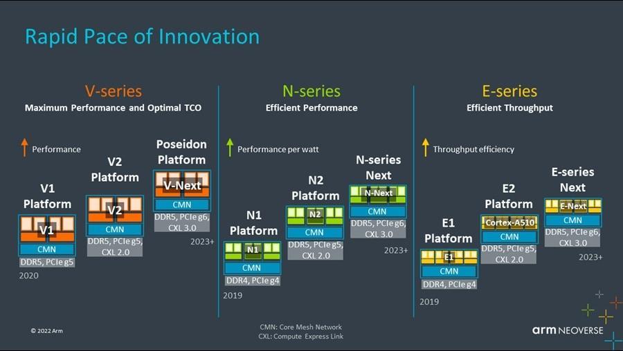
The above-mentioned Cadence JedAI Platform aims to shift EDA from single-run, single-engine algorithms to algorithms that leverage big data and artificial intelligence to optimize multiple runs of multiple engines across an entire SoC design and verification flow. With the JedAI Platform, Cadence is unifying big data analytics across its AI platforms – Verisium verification, Cerebrus implementation, and Optimality system optimization – as well as third-party silicon lifecycle management systems. Arm unveils Neoverse V2 Arm has unveiled the Neoverse V2 Platform (“Demeter”) featuring the newest V-series core and the Arm CMN-700 mesh interconnect. According to Arm, Neoverse V2 will deliver market-leading integer performance for cloud and HPC workloads; it also introduces several Armv9 architectural security enhancements. The company said it already has multiple partners with designs based on Neoverse V2 in progress, one of which is Nvidia for its Grace datacenter CPU. Arm is also developing the next generation of its N-Series and E-Series CPUs.
New fabs: Wolfspeed, Foxconn/Vedanta Wolfspeed will build a new 200mm silicon carbide wafer facility in Chatham County, North Carolina. The investment is targeted to generate a more than tenfold increase from Wolfspeed’s current silicon carbide production capacity on its Durham campus. Phase one construction is anticipated to be completed in 2024 and cost approximately $1.3 billion, with state and local incentives. A joint venture between Foxconn and Indian metals company Vedanta reportedly plans to build a chipmaking facility in India, in the Gujarat state. The total investment in the project – which includes semiconductor fabrication, assembly and testing as well as display production – is set to reach $19.4 billion. The Indian government will likely contribute a significant funding as part of an incentive plan. The planned venture is reportedly set to make chips using mature 28-nanometer technology. Artificial intelligence updates: PyTorch, MLPerf Meta (Facebook) has announced that the PyTorch framework for AI research will transition to a newly launched PyTorch Foundation, which will be part of the nonprofit Linux Foundation. MLCommons has recently published fresh results from MLPerf Inference v2.1 benchmarks, for both datacenter and edge applications. NIST and Google to help academic chip production The U.S. National Institute of Standards and Technology (NIST) has signed an agreement with Google to develop and produce chips targeted at research projects from academic institutions and startups. The chips will be manufactured by SkyWater Technology. Google will pay the initial cost of setting up production and will subsidize the first production run. NIST, with university research partners, will design the chips. The designs will be open source. Apple first to use TSMC’s N3E Apple reportedly aims to be the first company to use TSMC’s N3E (Enhanced) process, an upgraded version of the foundry’s current 3-nanometer technology. The Cupertino giant is planning to use N3E for its A17 mobile processor currently under development, which will power premium iPhones. The next generation of Apple’s M3 chip for Macs is also reportedly set to use the N3E process. Semiconductor process updates: EV Group, Cornell University Austria-based EV Group has introduced NanoCleave, a new layer release technology for silicon that enables ultra-thin layer stacking for front-end processing – an alternative to the commonly used 3D integration solution where temporary bonding is based on glass carriers and organic adhesives. With NanoCleave technology, the backside of the silicon wafer is exposed with an IR laser, which utilizes a wavelength that silicon is transparent to. An inorganic release layer – prebuilt into the silicon stack through standard deposition processes – absorbs the IR light, resulting in the cleaving of the silicon at a predetermined and precisely defined layer or area. Compared to organic adhesives, the inorganic release layers enable more precise and thinner release layers and withstand processing temperatures up to 1000°C, allowing layer transfer for many new front-end applications, such as epitaxy, deposition and annealing. A research team from Cornell University has developed a new microwave annealing technology enabling the use of microwave heating to obtain higher dopant concentration in silicon. Key to the new solution is the capability to selectively control standing waves inside the microwave oven, avoiding uneven dopant activation. To develop the new technology, researchers modified a regular household microwave oven. 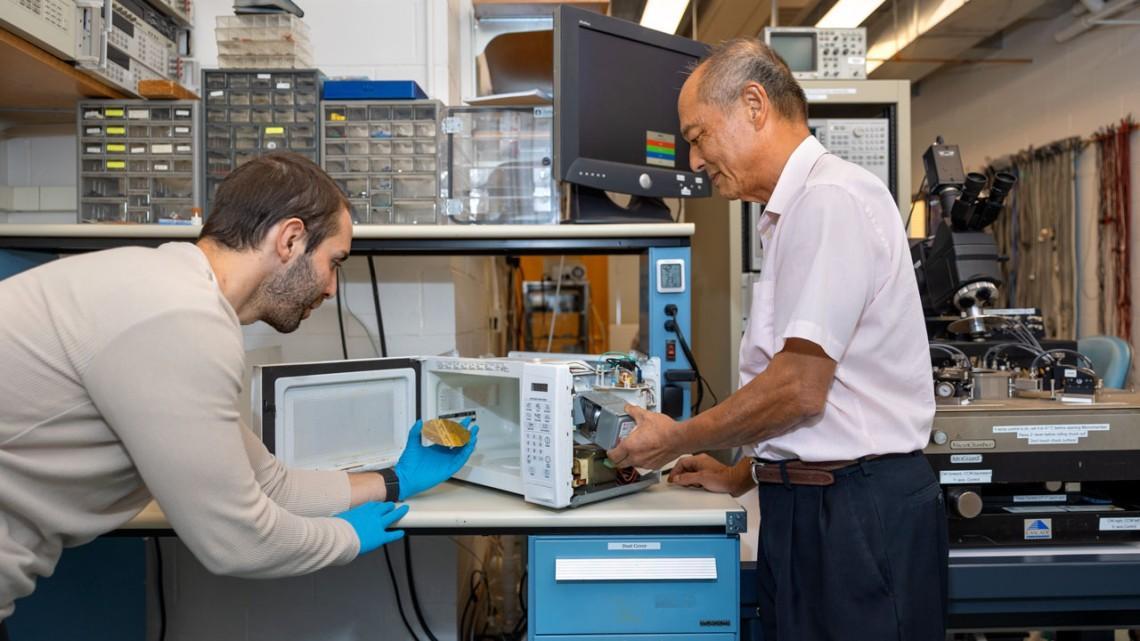 The Cornell University team working at the modified microwave oven. Credit: Ryan Young/Cornell University Risc-V in automotive applications: SiFive, Soc.one, Imagination SiFive has announced three Risc-V-based processors tailored for automotive applications: E6-A, X280-A, and S7-A. As the company stated in a press release, the new products are part of a long-term roadmap and portfolio designed to meet the specific needs of automotive manufacturers and their suppliers. An alliance between SoC.one and Imagination Technologies aims to accelerate the adoption of Risc-V in the automotive design cycle. SoC.one’s Cloud platform will be used to explore, design, build and train/validate Risc-V-based compute solutions in a ‘Digital Twins’ approach, with the goal of overcoming uncertainties around Risc-V maturity, performance, and security. Cruise (General Motors’ autonomous driving unit) is also reportedly “closely looking” at Risc-V. The company is developing its own chips for self-driving cars to be deployed by 2025. New car battery technology promises 600 miles range Michigan-based ONE (Our Next Energy) has unveiled a 240-Ah prismatic anode-free cell it believes is the highest energy density large-format cell ever produced. This will enable the commercialization of ONE’s Gemini dual-chemistry architecture, which will be integrated into a BMW iX prototype vehicle later this year. ONE’s solution involves two specialty chemistries in the same battery, with different functions: LFP (lithium iron phosphate) for daily driving, and anode-free to extend range for long distances. This combined system is expected to deliver more than 250,000 miles of lifetime service – and 600 miles of range. Wi-Fi updates: Intel, Broadcom, Ubilite Intel and Broadcom have recently showcased the industry’s first cross-vendor Wi-Fi 7 demonstration, with over-the-air speeds greater than 5 gigabits per second. The trial used an Intel Core processor-based laptop with a Wi-Fi 7 solution connected to a Broadcom Wi-Fi 7 access point. Ubilite has made available its UBI206 platform based on the UBI206 SoC, targeted specifically for ultra-low power wireless applications such as IoT. According to the company, UBI206 has a lower power consumption than Bluetooth. Upcoming events IPC Advanced Packaging Symposium – “Building the IC-Substrate and Package Assembly Ecosystem” will be held October 11-12 in Washington, D.C. Arm DevSummit is scheduled for October 26-27 in San Francisco. |
|
|
|||||
|
|
|||||
|
|||||


 Animation, 3D Art and 3D Models")