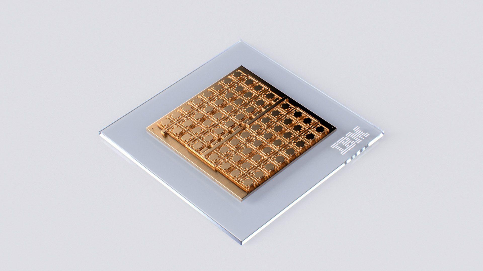
Unlike traditional integrated circuit (IC) designs, multi-dimensional 2.5D and 3D ICs are composed of multiple individual chiplets, each built to a separate process node best suited for its specific purpose. There are many different design options for connecting these chiplets, and any or all of these approaches can be combined on a single 3D IC assembly. This results in multiple components of different materials integrated in all three dimensions, which creates new and unique verification challenges for 2.5/3D IC designers.
3D IC assembly flow
Multi-dimensional ICs are one part of the industry’s answer to moving beyond the limits of Moore’s law. While 2.5D approaches, particularly chiplets placed upon a silicon interposer, have gained broad adoption, the move to true 3D IC is still early in its design lifecycle. Design tools and best design practices continue to evolve and improve, but many challenges are yet to be resolved.
In a true 3D IC, early design and package planning can be a challenging task, as the specific approach, materials, and chiplet placements used will induce thermal and mechanical stresses that can impact the intended electrical behavior of the full assembly design (Figure 1). Selecting the optimal approach and optimal chiplet placements becomes critical, implying multiple iterations will be required to determine the best final design.


