EDACafe Editorial Roberto Frazzoli
Roberto Frazzoli is a contributing editor to EDACafe. His interests as a technology journalist focus on the semiconductor ecosystem in all its aspects. Roberto started covering electronics in 1987. His weekly contribution to EDACafe started in early 2019. Research in electronic devices takes center stage at 2020 IEDM eventDecember 7th, 2020 by Roberto Frazzoli
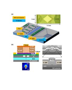
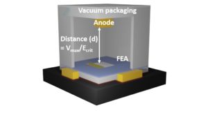
Running as a virtual event from Saturday through Friday, December 12-18, this years’ edition of IEDM (IEEE International Electron Devices Meeting) will offer a mix of live-streamed video content (such as the plenary presentations, panel discussion and career session) and on-demand pre-recorded presentations, with a schedule of live Q&A sessions. The event’s program includes more than 220 papers, plus tutorials and short courses. Part of the papers will cover emerging topics through six focus sessions: cryogenic electronics; GaN and SiC; future interconnect; technologies enabling 5G and beyond; energy harvesting and wireless power transmission; DTCO of advanced logic and memory. As a quick preview of the event, let’s now have a look at some of the technical highlights from the presentations. Intel’s future transistor: stacked NMOS-on-PMOS nanoribbons Next generation FET architectures for logic devices are a much-debated issue in the industry, and at IEDM Intel researchers will present a new candidate: a NMOS-on-PMOS transistor built from multiple self-aligned stacked nanoribbons. This architecture employs a vertically stacked dual source/drain epitaxial process and a dual metal gate fabrication process, enabling different conductive types of nanoribbons to be built so that threshold voltage adjustments can be made for both top and bottom nanoribbons. According to Intel, this approach combines excellent electrostatics (subthreshold slope of <75 mV/dec) and DIBL (Drain Induced Barrier Lowering, <30mV/V for gates ≥30nm) with a path to significant cell size reduction due to the self-aligned stacking. These devices were used to build a functional CMOS inverter with well-balanced voltage transfer characteristics. 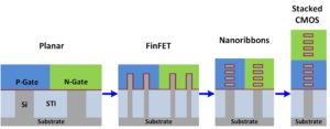 The evolution of transistor architectures from planar, to FinFETs, to nanoribbons and to a 3D CMOS architecture. Credit: Intel Molybdenum disulfide transistors Besides new architectures, transistor research also concerns the use of new materials. At IEDM, Belgian research institute Imec will report about the results of a study on transistors made of molybdenum disulfide (MoS2), a material that promises better control of electrostatics than silicon in FinFETs – and hence better immunity to short-channel effects, a significant performance issue at smaller dimensions. Imec researchers performed the first study of variability in nanoscale MoS2. Samsung’s single-chip lidar One of the hurdles on the road to fully autonomous vehicles is the high cost of sensors. As for lidars, a potentially lower cost option will be presented by Samsung researchers, who have come up with the first single-chip lidar beam scanner. According to Samsung, the new device opens the possibility of ultra-low cost, compact lidar systems because it requires no separate light source – unlike current systems which are larger and use mechanical beam scanners with motors and rotating mirrors. The single-chip lidar integrates a fully functional 32-channel optical phased array, 36 optical amplifiers, and tunable laser diode onto a 7.5x3mm2 die, fabricated with III-V-on-Si processes. Also, a calibration algorithm based on machine-learning is used in digital signal processing for real-time operation. The device achieved real-time 20 frames-per-second operation, at a resolution of 120 x 20 lines, at 10 meters. Memory advancements: denser DRAM, automotive grade PCM Another Intel team will discuss the use of the antiferroelectric (AFE) material hafnium-zirconium-oxide (HfZrO2) to make a 3D deep-trench capacitor for potential use in embedded DRAM memories. It demonstrated endurance of 1012 cycles even at high temperatures, and a 1.8V operating voltage. The researchers used these AFE capacitors in a novel memory architecture for ultra-high bit density: a vertical stack based on one access transistor with multiple AFE capacitors in parallel. Each capacitor represents a single memory bit. A significant density boost was achieved by stacking four AFE capacitors in a vertical fashion, with no area increase. 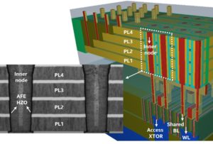 The AFE-based embedded DRAM: cross-sectional TEM image of stacked vertical capacitors, along with a cross-sectional representation of the memory architecture. Credit: Intel And a team comprising researchers from STMicroelectronics and from French institute CEA-Leti will present an ultra-dense embedded phase-change memory technology (cell size = 0.019µm2) for automotive SoCs that meets the AEC-Q100 Grade 0 standard. It leverages a 28nm FDSOI substrate; novel super-shallow trench isolation for the bit line (requiring no trench etch-and-fill); high-voltage (5V) triple-gate-oxide transistors; and a compact bipolar junction transistor selector. 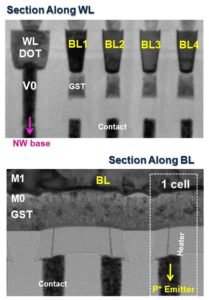 A TEM cross-section of the automotive-grade, FDSOI-based embedded PCM. Credit: STMicroelectronics and CEA-Leti Silicon vacuum transistor challenges GaN and SiC on high voltages Moving to power applications, a team led by MIT researchers will describe the first silicon vacuum transistor operating at ~40 kV, a voltage level normally achieved by wide-bandgap materials like SiC and GaN. The proof-of-concept device consists of an electron source (a gated field emission array or FEA), a vacuum drift region and a metal anode. Electrons emitted by the source travel through the vacuum and are collected at the anode. The vacuum determines the transport properties and the high-voltage isolation. According to the researchers, this technology can lead to compact, high-performance vacuum devices able to outperform solid-state devices on all metrics, making them suitable for a range of high-power and high-frequency applications, and also as next-generation X-ray sources. Exploiting the GaN potential: new rectifiers, 20GHz transistors But gallium nitride still has potential to be exploited, in power and high-frequency applications. A team led by Virginia Tech researchers will describe the first multi-kV operation of lateral AlGaN/GaN Schottky barrier diodes. Built on 4-inch GaN-on-sapphire wafers, the devices consist of a stack of five parallel 2DEG (two-directional electron gas) channels in combination with a fin-based 3D anode structure which wraps the p-n junction around the fins. The diodes demonstrated a 5.2 kV breakdown voltage, a low specific on-resistance (13.5 mΩ·cm2), and low off-state leakage current, leading to a 2 GW/cm2 figure of merit which surpasses that of unipolar SiC Schottky barrier diodes. 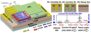 A 3D schematic of the multi-channel AlGaN/GaN Schottky barrier diode. Credit: Virginia Polytechnic/UCLA/Enkris Semiconductor/Qorvo And a team comprising Cornell and Intel researchers will present the first GaN-based p-channel HFETs to break the GHz frequency barrier. The devices take advantage of the polarization-induced 2D “hole gas” (holes free to move in two dimensions) found in the GaN/AlN heterostructure. The researchers will report that with a scaled source/drain distance and gate length, and low-resistance ohmic contacts, p-channel GaN HFETs demonstrated On currents >420 mA/mm and fT/fMAX~20 GHz. According to the team, these new results can take this wide-bandgap CMOS platform into new RF and power applications. 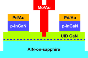 GaN-based p-channel transistor: schematic of the Mo/Au Schottky T-gate. Credit: Cornell University/Intel More technical highlights from this years’ IEDM program include the first 300mm platform for design of qubits for quantum computing, from Belgian research institute Imec; a high-density logic-on-logic 3D IC design from Arm and Globalfoundries; a large-area digital microfluidics platform based on the thin-film transistor technology used in flat-panel displays, from the Chinese Academy of Sciences; etc. |
|
|
|||||
|
|
|||||
|
|||||


