Open side-bar Menu
 EDACafe Editorial

Archive for December, 2020

2020 year in review

Thursday, December 31st, 2020

Needless to say, the Covid-19 pandemic turned 2020 into a nightmare. It also changed most people’s working life, shutting down in-person gatherings and replacing them with virtual events. Still, 2020 was an exciting year for the semiconductor industry and related segments – in terms of market growth, technological innovation, and overall evolution. As we approach the year’s end, let’s try to briefly summarize some of the major events and themes that characterized the last twelve months.

Credit: yavuzunlu – depositphotos.com

A record year for acquisitions

The most apparent characteristic of 2020 was definitely the large number of sizeable acquisitions, either announced or completed. This obviously refers to the Nvidia-Arm, AMD-Xilinx, Analog Devices-Maxim and Infineon-Cypress deals, but also to many other smaller yet significant acquisitions. During 2020, EDACafe reported about approximately fifty of them.

(more…)

Risc-V Summit 2020 showcases a growing ecosystem and a wider application spectrum

Monday, December 14th, 2020

The virtual event held from December 8 to 10 offered several updates on topics such as core design verification, standard extensions enabling new applications, and open-source EDA tools, with contributions from both the industry and academic research

Almost one quarter (23 percent) of all new IC/ASIC or FPGA projects incorporate a Risc-V processor in their design, according to the 2020 Wilson Research Group functional verification study, a survey – available here and here – commissioned by Mentor. In fact, 2020 has been a year of growth for this open instruction set architecture, as underlined by Calista Redmond, CEO of Risc-V International, in her keynote at this year’s Risc-V Summit. Adoption has grown in all industry segments, including embedded, AI, IoT, HPC etc. Initiatives carried out by Risc-V International in 2020 include ratification of the processor trace specification, a new algorithm that allows to see what instructions a core is executing; a partnership with GlobalPlatform, the standard for secure digital services and devices; new alliances, training programs, and more.

The association also launched the ‘Risc-V Exchange’, with more than 124 Risc-V cores and SoCs and developer boards along with 129 Risc-V software applications and tools. Plans for 2021 include public review for several new standard extensions. Let’s now take a quick look at some of the innovations presented at the Summit. All the papers briefly quoted here can be accessed from the event website.

(more…)

Research in electronic devices takes center stage at 2020 IEDM event

Monday, December 7th, 2020

Running as a virtual event from Saturday through Friday, December 12-18, this years’ edition of IEDM (IEEE International Electron Devices Meeting) will offer a mix of live-streamed video content (such as the plenary presentations, panel discussion and career session) and on-demand pre-recorded presentations, with a schedule of live Q&A sessions. The event’s program includes more than 220 papers, plus tutorials and short courses. Part of the papers will cover emerging topics through six focus sessions: cryogenic electronics; GaN and SiC; future interconnect; technologies enabling 5G and beyond; energy harvesting and wireless power transmission; DTCO of advanced logic and memory. As a quick preview of the event, let’s now have a look at some of the technical highlights from the presentations.

Intel’s future transistor: stacked NMOS-on-PMOS nanoribbons

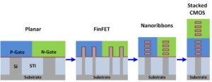
Next generation FET architectures for logic devices are a much-debated issue in the industry, and at IEDM Intel researchers will present a new candidate: a NMOS-on-PMOS transistor built from multiple self-aligned stacked nanoribbons. This architecture employs a vertically stacked dual source/drain epitaxial process and a dual metal gate fabrication process, enabling different conductive types of nanoribbons to be built so that threshold voltage adjustments can be made for both top and bottom nanoribbons. According to Intel, this approach combines excellent electrostatics (subthreshold slope of <75 mV/dec) and DIBL (Drain Induced Barrier Lowering, <30mV/V for gates ≥30nm) with a path to significant cell size reduction due to the self-aligned stacking. These devices were used to build a functional CMOS inverter with well-balanced voltage transfer characteristics.

The evolution of transistor architectures from planar, to FinFETs, to nanoribbons and to a 3D CMOS architecture. Credit: Intel


(more…)


© 2024 Internet Business Systems, Inc.
670 Aberdeen Way, Milpitas, CA 95035
+1 (408) 882-6554 — Contact Us, or visit our other sites:
TechJobsCafe - Technical Jobs and Resumes EDACafe - Electronic Design Automation GISCafe - Geographical Information Services  MCADCafe - Mechanical Design and Engineering ShareCG - Share Computer Graphic (CG) Animation, 3D Art and 3D Models
  Privacy PolicyAdvertise