


EDACafe Editorial Roberto Frazzoli
Roberto Frazzoli is a contributing editor to EDACafe. His interests as a technology journalist focus on the semiconductor ecosystem in all its aspects. Roberto started covering electronics in 1987. His weekly contribution to EDACafe started in early 2019. EDA updates; new generation Nvidia GPU; research on AI energy savings; future Tesla batteriesMay 22nd, 2020 by Roberto Frazzoli
News related to artificial intelligence abound this week – including a notable research work that promises to reduce training energy consumption up to one-tenth. Before proceeding to this week’s news roundup, let’s briefly mention that – as widely reported by the media – on May 15th TSMC announced its intention to build and operate a 5-nanometer fab in Arizona. The news has spurred a lot of comments, such as the ones reported in this EETimes article. EDA updates: Cadence, Mentor, Synopsys Cadence has made available ten new Verification IP (VIP) solutions supporting the development of SoCs and microcontrollers for automotive, hyperscale data center and mobile applications, including CXL, HBM3, TileLink and MIPI CSI‑2sm 3.0. Also available from Cadence, a 56G long-reach SerDes IP on TSMC’s N7 and N6 process technologies. And on its part, TSMC has granted certifications for its N5 and N6 process technologies to Mentor – for a broad array of IC design tools – and to Synopsys – for digital and custom design platforms.
The new 54-billion transistor Nvidia GPU Brilliant startups around the world keep on inventing brilliant new AI acceleration architectures, often advertising their performances in comparison with Nvidia GPUs. The race obviously doesn’t stop, as Nvidia GPU performance is a moving target: the recently announced EGX A100 Nvidia chip, based on the new Ampere architecture, has significantly raised the bar. With 54 billion transistors, the A100 is – according to Nvidia – the largest 7 nanometer chip ever built, and this enormous budget has been used to introduce several innovations contributing to a sharp performance increase compared to previous generations. Here is an extremely quick summary. Third-generation tensor cores bring two new precision formats, Tensor Float 32 (TF32) and Floating Point 64 (FP64), providing additional acceleration; the Multi-Instance GPU feature (MIG) allows each A100 processor to be partitioned in up to seven virtualized GPU instances; third-generation NVLink doubles the GPU-to-GPU direct bandwidth to 600 gigabytes per second, and when paired with the latest generation of NVSwitch allows all GPUs in the server to talk to each other at full NVLink speed; the tensor cores’ support for “sparsity” – a typical characteristic of neural network workload – can provide up to 2X higher performance for sparse AI models; memory bandwidth has been increased to 1.6 terabytes per second, and on-chip memory now includes a 40 megabyte level 2 cache; lastly, A100 features Mellanox’s ConnectX-6 Dx SmartNIC to further increase acceleration capabilities. Details about the A100 and the Ampere architecture can be found in this 83-page white paper. 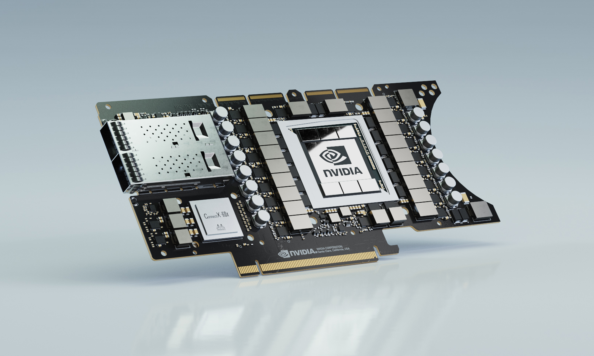 Nvidia EGX A100 converged accelerator. Image credit: Nvidia AI industry news: Microchip, Sony, InspireSemi, Tachyum Making it easier for software developers to implement their neural network algorithms on FPGAs, without prior FPGA design experience: after Xilinx’ Vitis and Intel’s oneAPI, Microchip is now offering a similar capability – for embedded vision applications – with its new VectorBlox Accelerator SDK targeted at PolarFire FPGAs. Besides enabling developers to code in C/C++, the toolkit can execute models in TensorFlow and in the ONNX format which supports many frameworks such as Caffe2, MXNet, PyTorch, and MATLAB. Speaking of vision applications, Sony has developed two “intelligent vision sensors” equipped with AI processing functionality, obtained by a stacked configuration consisting of a pixel chip and a logic chip. Local AI processing of video images enables cameras – for example – to count the number of visitors entering a facility, detect stock shortages in a shop, detect gathering of people etc. As for new processing architectures, InspireSemi (Austin, Texas) has developed its second-generation ASIC solution for Artificial Intelligence, blockchain and scientific high performance computing. InspireSemi’s processor architecture is based on an array of thousands of simple CPU cores, tightly integrated with memory and networking through a proprietary on-chip network. One more chip update: startup Tachyum has completed the layout of its Prodigy Universal Processor, with a verified detailed physical design of more than 90 percent of the silicon area. 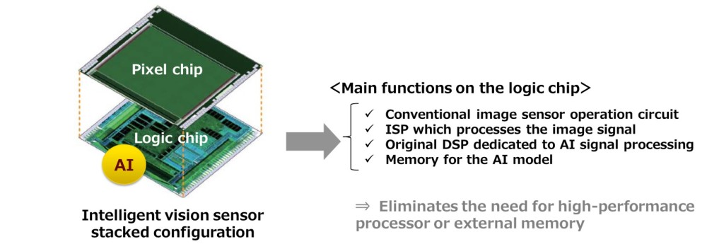 The stacked configuration of Sony’s intelligent vision sensors. Image credit: Sony AI research news: Rice University, IBM Up to 5.8x – 10.7x energy savings in training while maintaining comparable or even better accuracy: this is the promise of a technique based on early identification of “winning tickets”, developed by a research team from Rice University (Houston, Texas). As the authors recall in their paper, previous researches have shown that neural networks hide “winning tickets”, small but critical subnetworks that can be trained alone to reduce the training effort; however, up until now their identification still required the costly train-prune-retrain process. The Rice University team has discovered that the winning tickets can be identified at a very early training stage via low cost training schemes, and – what’s more – that efficient training based on early discovered tickets can achieve dramatic energy savings. IBM Research, too, is exploring ways to cut AI hardware power consumption – as recently reported by EDACafe. As for inference, an example of this work is a study on in-memory computing based on phase-change memory (PCM). Key finding of this research is a way to retain accuracy despite PCM less-than-ideal performance, including device variability and read/write conductance noise. To overcome this, the team injected noise to the synaptic weights during the training of DNNs in software. This resulted in no considerable accuracy loss when transferring weights to PCM devices. Tesla’s future batteries expected to bring EV cost in line with gasoline models Tesla is reportedly planning “to introduce a new low-cost, long-life battery in its Model 3 sedan in China later this year or early next that it expects will bring the cost of electric vehicles in line with gasoline models.” Battery cost reduction would be achieved through a combination of low-cobalt or cobalt-free chemistries, heavily automated manufacturing processes, and the possibility to reuse EV batteries in the electric power grid. May events: 2019 vs 2020 One year ago EDACafe briefly reported about several “real” events from both IT giants and silicon related companies – Facebook, Microsoft, Google, Samsung Foundry, Intel, Imec – all taking place in May. This year the Covid-19 pandemic has obviously impacted those events. Facebook F8 2020 has been cancelled and replaced by “a series of updates throughout the year” from Mark Zuckerberg and other Facebook leaders; Microsoft Build 2020 took place as a virtual event on May 19 and 20; Google I/O 2020 was just cancelled, with no replacement – not even in a virtual format; Samsung Foundry Forum has been “postponed to the second half of the year”; Intel 2020 Annual Stockholders’ Meeting was held as a virtual event; and Imec’s Future Summits have been cancelled, with next edition scheduled for May 11-12, 2021. |
|
|
|||||
|
|
|||||
|
|||||


 Animation, 3D Art and 3D Models")