


The Dominion of Design Sanjay Gangal
Sanjay Gangal is a veteran of Electronics Design industry with over 25 years experience. He has previously worked at Mentor Graphics, Meta Software and Sun Microsystems. He has been contributing to EDACafe since 1999. Unravelling the mind-body connection with power-efficient IC chip jointly developed by A*STAR IME, NTU and NUSNovember 25th, 2013 by Sanjay Gangal
Article source: IME Despite the advances in neuroscience research, the human brain remains a complex puzzle with questions unanswered on how it controls human behaviour, cognitive functions and movements. Scientists from A*STAR Institute of Microelectronics (IME), Nanyang Technological University (NTU) and National University of Singapore (NUS) have jointly developed and demonstrated an integrated circuit (IC) chip with record-low power consumption for direct recording of brain activities. This breakthrough minimises the patient’s exposure to electromagnetic radiation and heat during the recording process, making it possible to integrate greater number of channels (>100 channels) to acquire more comprehensive profile of brain signals, paving the way to unlock the mystery behind the complex mind-body connection. Neural recording system is a vital tool to acquire and process brain signals, and is also applied in artificial limb control (or neural prosthesis) treatments for paralyzed patients. The system comprises multiple electrodes for data acquisition and is implanted within the skull during the operation. The implantability of the system places tight limits on its size and power consumption, while at the same time demanding sufficient performance to record good quality data. Using Simulation to Optimize Safety, Performance, and Cost Savings When Integrating an Antenna Onto a PlatformFebruary 7th, 2013 by Sanjay Gangal
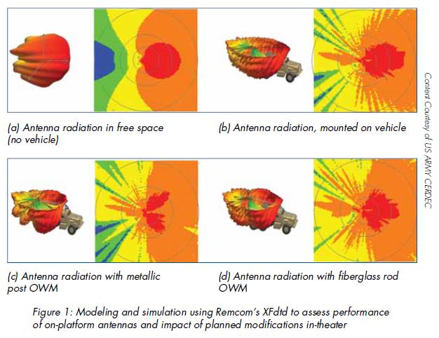
Article source: Remcom Successful integration of an antenna onto a vehicle platform poses many challenges. Vehicle features impact antenna performance by blocking, reflecting or reradiating energy, and co-site interference can impair the effectiveness of multi-antenna configurations. Platform motion and environmental factors such as terrain and buildings may reduce system effectiveness in actual op The key benefit of simulation-based assessment is that it is relatively fast and cost-effective compared to physical system modification and measurement. The lead times and costs associated with scheduling measurements in an anechoic chamber or at an outdoor test facility sometimes strain schedules and budgets. Modeling and simulation can assess options and tradeoffs in order to select a small number of planned approaches well before any physical testing occurs; as a result, experimental design focuses on verifying planned approaches and fine-tuning alternatives demonstrated to be effective in simulations. This approach reduces the risk of encountering problems that require retesting, costly redesign or introduce dangerous in-theater behavior. In addition, a number of challenges arise when attempting to perform exhaustive laboratory or field testing on an integrated system. Some potential issues include:
A comprehensive modeling and simulation toolset allows an organization to overcome these challenges by being able to simulate any number of conditions, identify and resolve key issues, and reserve the use of physical measurements to confirm successful pre-test, simulation-based assessments. The remainder of this article provides several examples demonstrating typical simulation-based assessments to identify and resolve issues related to antenna performance and integration onto vehicles.
MIT researchers improve quantum-dot performanceFebruary 4th, 2013 by Sanjay Gangal
Written by: David L. Chandler, MIT News Office New production method could enable everything from more efficient computer displays to enhanced biomedical testing. CAMBRIDGE, Mass. — Quantum dots — tiny particles that emit light in a dazzling array of glowing colors — have the potential for many applications, but have faced a series of hurdles to improved performance. But an MIT team says that it has succeeded in overcoming all these obstacles at once, while earlier efforts have only been able to tackle them one or a few at a time.  Moungi G. Bawendi Quantum dots — in this case, a specific type called colloidal quantum dots — are tiny particles of semiconductor material that are so small that their properties differ from those of the bulk material: They are governed in part by the laws of quantum mechanics that describe how atoms and subatomic particles behave. When illuminated with ultraviolet light, the dots fluoresce brightly in a range of colors, determined by the sizes of the particles. First discovered in the 1980s, these materials have been the focus of intense research because of their potential to provide significant advantages in a wide variety of optical applications, but their actual usage has been limited by several factors. Now, research published this week in the journal Nature Materials by MIT chemistry postdoc Ou Chen, Moungi Bawendi, the Lester Wolfe Professor of Chemistry, and several others raises the prospect that these limiting factors can all be overcome. The new process developed by the MIT team produces quantum dots with four important qualities: uniform sizes and shapes; bright emissions, producing close to 100 percent emission efficiency; a very narrow peak of emissions, meaning that the colors emitted by the particles can be precisely controlled; and an elimination of a tendency to blink on and off, which limited the usefulness of earlier quantum-dot applications. Read the rest of MIT researchers improve quantum-dot performance Cadence, ARM and Samsung Tapeout Industry’s First Cortex-A-Based 14nm/FinFET ChipDecember 20th, 2012 by Sanjay Gangal
ARM (LSE: ARM) (NASDAQ: ARMH) and Cadence Design Systems, Inc. (NASDAQ: CDNS) announced the tape-out of the first 14-nanometer test chip implementation of the high-performance ARM® Cortex™-A7 processor, the most energy-efficient applications processor from ARM. Designed with a complete Cadence® RTL-to-signoff flow, the chip is the first to target Samsung’s 14-nanometer FinFET process, accelerating the continuing move to high-density, high-performance and ultra-low power SoCs for future smartphones, tablets and all other advanced mobile devices.
Read the rest of Cadence, ARM and Samsung Tapeout Industry’s First Cortex-A-Based 14nm/FinFET Chip “Kilopass Roadmap for Advanced TSMC Processes” by Harry Luan, CTO at Kilopass TechnologyNovember 5th, 2012 by Sanjay Gangal
Article source: Kilopass Technology “Kilopass Roadmap for Advanced TSMC Processes” by Harry Luan, chief technology officer at Kilopass Technology Inc., was presented at the 2012 TSMC Open Innovation Platform Ecosystem Conference on Tuesday, October 16, at 4:30 p.m. in the San Jose Convention Center, San Jose, California. Kilopass is a leading provider of semiconductor logic non-volatile memory (NVM) intellectual property (IP).
“Novel New Vertically-Oriented, Antifuse Non-Volatile Memory Bit Cell” by Harry Luan, CTO of Kilopass TechnologyOctober 22nd, 2012 by Sanjay Gangal
Article source: Kilopass Technology Harry Luan, chief technology officer at Kilopass Technology Inc., a leading provider of semiconductor logic non-volatile memory (NVM) intellectual property (IP) presenting “Novel New Vertically-Oriented, Antifuse Non-Volatile Memory Bit Cell” at MemCon 2012 on Tuesday, September 18, at 2:15 p.m. at the Santa Clara Convention Center, Santa Clara, Calif. The new embedded VCM (Vertical Cross-point Memory) NVM IP bit cell quadruples the density of today’s anti-fuse NVM IP bit cell. The VCM bit cell will make possible program storage where today’s embedded non-volatile memory (eNVM) technology is cost-prohibitive or unavailable at capacities of 4Mb to 32Mb. It will also enable a higher level of performance more similar to SRAM compared to existing slower eNVM technologies or external flash or EEPROM chips.
‘Invisibility’ could be a key to better electronicsOctober 11th, 2012 by Sanjay Gangal
Author: David Chandler, MIT News Office MIT team applies technology developed for visual ‘cloaking’ to enable more efficient transfer of electrons. A new approach that allows objects to become “invisible” has now been applied to an entirely different area: letting particles “hide” from passing electrons, which could lead to more efficient thermoelectric devices and new kinds of electronics. The concept — developed by MIT graduate student Bolin Liao, former postdoc Mona Zebarjadi (now an assistant professor at Rutgers University), research scientist Keivan Esfarjani, and mechanical engineering professor Gang Chen — is described in a paper in the journal Physical Review Letters.  Diagram shows the 'probability flux' of electrons, a representation of the paths of electrons as they pass through an 'invisible' nanoparticle. While the paths are bent as they enter the particle, they are subsequently bent back so that they re-emerge from the other side on the same trajectory they started with — just as if the particle wasn't there. - Image courtesy Bolin Liao et al. Normally, electrons travel through a material in a way that is similar to the motion of electromagnetic waves, including light; their behavior can be described by wave equations. That led the MIT researchers to the idea of harnessing the cloaking mechanisms developed to shield objects from view — but applying it to the movement of electrons, which is key to electronic and thermoelectric devices. Read the rest of ‘Invisibility’ could be a key to better electronics The Measure of Nanometer Silicon SuccessSeptember 24th, 2012 by Graham Bell
I was speaking with experts at Mentor about the latest developments in back-end physical verification (PV) and design-for-manufacturing (DFM). It prompted me to take a look at what has changed and what will be essential going forward. Here is what I see for this critical area for IC implementation. First, we have passed the 28nm barrier and are already looking to a new generation of design. Leading-edge design starts are now at 20nm and we will see production silicon for that node by early 2013. However, in a new research brief, “Driving first-time silicon success across the IC ecosystem,” by Dr. Handel Jones, semiconductor analyst at IBS, the total number of design starts is not growing. While System integrators such as Samsung and Apple, are furiously growing their mobile businesses, the ability to integrate ever-larger collections of IP in their SOCs means they do not need to include more ICs in their phones to expand the features of their products. It is also true that 20nm designs have a much higher NRE than previous generations. Naturally, this economic incentive will keep some design starts at the 28nm and larger nodes. ASQED 2012 in Malaysia a huge success!July 31st, 2012 by Sanjay Gangal
Article source: ASQED ASQED 2012 was held on July 10-11 at Penang, Malaysia. The 4th Asia Symposium on Quality Electronic Design (ASQED 2012) was the fourth event organized by the International Society for Quality Electronic Design with technical sponsorship from several IEEE Societies. This event was sponsored and managed by SHRDC. ASQED emphasizes innovations and the latest developments in System and IC Design, MEMS & NEMS, Semiconductor Technology & Manufacturing, IC Packaging & PCB Technology, Test, and Bio & Nano Electronics.  ASQED Microelectronic Olympiad winner received the award from Rich Goldman of Synopsys. From left: Prof. Amin Bermak, Dr. Ali Iranmanesh, Mr. Rich Goldman, Mr. Reza Asadpour, Prof. Osseiran. The World of Drama and the Verification Engineer – A High Schooler’s PerspectiveJune 28th, 2012 by Shachi Nandan Kakkar
Before I step on stage for a performance, I look at the crowd and say, “Lord, please don’t let me screw this up.” But it is the effort before this performance that really leads to this moment. First we have a casting process, where we try to find the best actor to play the lead, then the understudy, then the extras and technical team etc. This is usually done by a director, someone who has excelled at acting before, and develops the entire vision. Then we memorize our lines, this is the most mind-numbing and difficult part, so to prevent mental break downs, we divide the script up into smaller parts. We start with a few simple lines, then progressively add more lines and difficulty of memorization. Then we block the entire play, see what goes where, and perform it. Next, we have dress rehearsals, we get comfortable performing in our costumes and make sure things go off without a hitch. Now after all of this, we present it to the audience and hope that we don’t get pelted with tomatoes. After we perform, we wait for the audience to react, if they respond with cheers, we repeat the act the same way the next night with minor adjustments, if we are hurt and killed with articles of food, we then see what to improve and make changes for the next show. Read the rest of The World of Drama and the Verification Engineer – A High Schooler’s Perspective |
|
|
|||||
|
|
|||||
|
|||||


 Animation, 3D Art and 3D Models")