


EDACafe Editorial Roberto Frazzoli
Roberto Frazzoli is a contributing editor to EDACafe. His interests as a technology journalist focus on the semiconductor ecosystem in all its aspects. Roberto started covering electronics in 1987. His weekly contribution to EDACafe started in early 2019. EDA Q3 2022 numbers; new PCB SI tools; chiplet description standard; FPGA applications; WiFi-based imagingJanuary 26th, 2023 by Roberto Frazzoli
Tech giants have been in the news over the past few days for a wave of workforce reductions: the list includes Alphabet (Google), Amazon, Microsoft, Meta (Facebook), and IBM. In at least two cases, these cost-cutting moves are accompanied by new investments in artificial intelligence: Alphabet reportedly plans to double down on AI, and Microsoft has just announced the third phase of its long-term partnership with OpenAI through a multiyear, multibillion dollar investment. Let’s now move to this week’s news roundup, starting with some EDA updates. EDA industry Q3 2022 numbers According to the latest report from the ESD Alliance, the Electronic System Design industry revenue increased 8.9% from $3,458.2 million in Q3 2021 to $3,767.4 million in Q3 2022. The four-quarter moving average, which compares the most recent four quarters to the prior four, rose 13.4%. Exceptions to these good results are the Semiconductor Intellectual Property (SIP) product category, with a 1% revenue decrease, and the Japan region with an 8.5% revenue decline. The EMEA region (Europe, Middle East, and Africa) reported just a 0.2% increase in Q3 2022. New PCB signal integrity tools from Keysight and Avishtech Keysight has introduced the Electrical Performance Scan (EP-Scan), a new high-speed digital simulation tool that supports rapid signal integrity analysis for hardware engineers and printed circuit board designers. According to the company, uncertainty about the length of the SI analysis phase performed by SI specialists creates a bottleneck in the PCB design cycle and delays time-to-market. EP-Scan addresses SI analysis bottlenecks by giving hardware designers diagnostic tools to correct designs earlier and meet development schedules. Avishtech has launched two new low-cost toolsets, Gauss SI and SI Pro, to rapidly construct PCB stackups and simulate for impedance and loss. According to the company, up until now these capabilities were only available to large corporations, who could afford very expensive software, whereas Gauss SI and SI Pro enable every board designer and engineer to specify their stackup and design for impedance and signal integrity. 2022 Year in ReviewJanuary 22nd, 2023 by Roberto Frazzoli
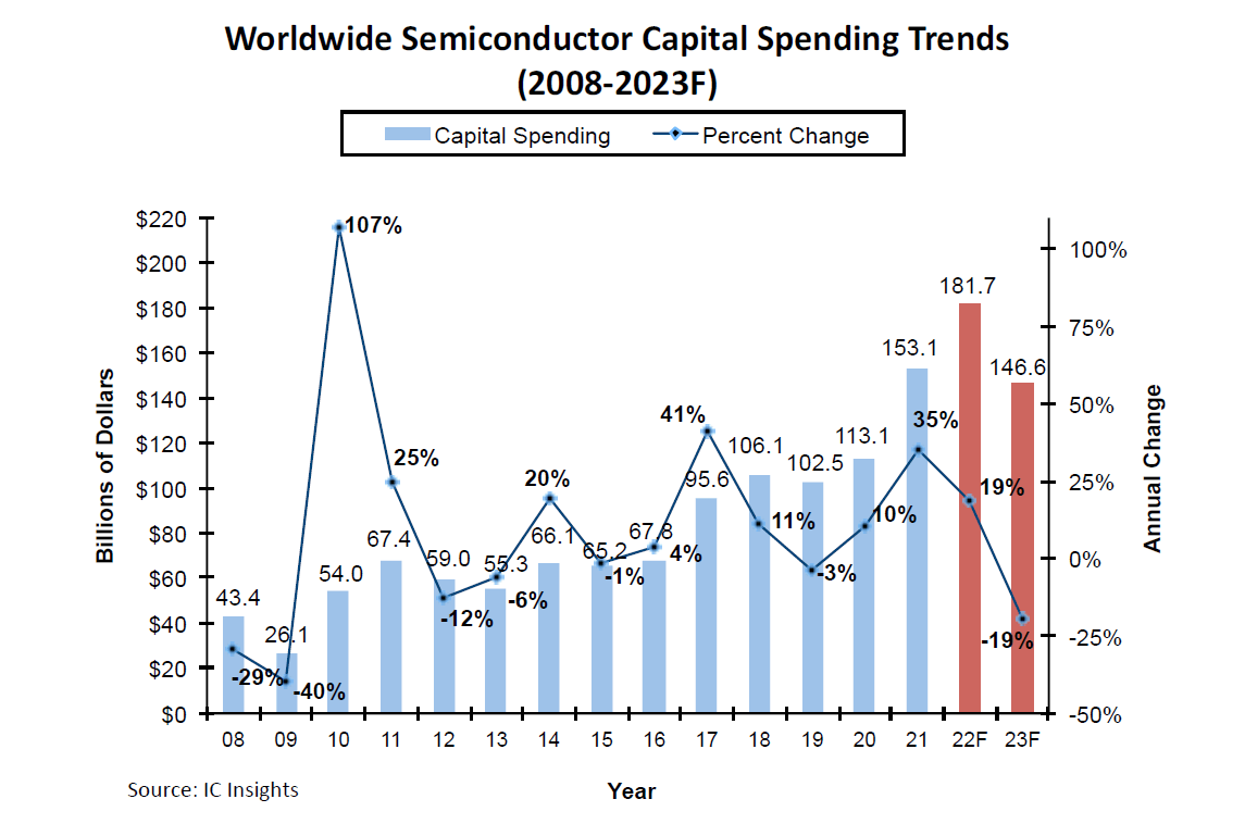
Let’s start the new year with a quick recap of some of 2022 events and trends. A year marked by three significant anniversaries – the transistor, the microprocessor and AlexNet turning 75, 50, and 10, respectively – 2022 was also characterized by a dramatic and unexpected change of the global geopolitical and economic climate. War in Ukraine, the spike in energy prices, and inflation shaped a new scenario. From chip shortage to capex drop At the beginning of 2022 “the” problem was the chip shortage forcing several carmakers to halt their assembly lines, with governments asking foundries to increase capacity. Just a few months later, several chipmakers cut their planned capital expenditure citing weaker consumer demand. Among them Taiwanese foundry UMC, and South Korean memory maker SK hynix, which decided to cut its investment next year by more than 50% due to the deterioration of the memory market conditions. Market research firm IC Insights forecasts a -19% drop in total worldwide semiconductor capital industry spending in 2023. An unprecedented amount of subsidies In 2022, the escalation in geopolitical tensions – especially between the U.S. and China – prompted governments around the world to subsidize their domestic semiconductor industry, with the goal of gaining independence. An unprecedented amount of taxpayers’ money is set to benefit qualified applicants over the next few years: $52.7 billion in the U.S. (CHIPS and Science Act), $45 billion in the European Union (EU Chips Act), $10 billion in India. Adding to this, the Japanese government will subsidize the newly established Rapidus chipmaker company. On the other side of the barricade, China is reportedly working on a $143 billion support package for its semiconductor industry. As for the U.S., 2022 saw the birth of two initiatives related to geopolitical tensions (America’s Frontier Fund) and to subsidies (American Semiconductor Innovation Coalition). CDC standard; PDF-proteanTecs collaboration; TSMC 3nm ceremony; new chips for Apple and DellJanuary 19th, 2023 by Roberto Frazzoli
Catching up on some of the latest news after seasonal holidays – but skipping the CES announcements overload – let’s start by briefly mentioning the recent Risc-V Summit where a Google executive spoke about Google’s support for the porting of Android to Risc-V: here’s the video of the speech. Accellera to develop a Clock Domain Crossing standard Accellera has announced the formation of the Clock Domain Crossing (CDC) Working Group, with the goal of defining a standard CDC collateral specification to ease SoC integration. Currently, lack of standard means that different CDC verification tools generate incompatible IP-level CDC collateral. This scenario is causing a CDC verification problem when the SoC teams source IP from IP providers that use a different tool for their own CDC verification. PDF Solutions and proteanTecs to collaborate on analytics-telemetry solutions PDF Solutions, a provider of semiconductor data analytics, and proteanTecs, a specialist of on-chip telemetry, have announced a collaboration on combined solutions intended to provide deeper insights on semiconductor yield, quality and reliability. The collaboration includes PDF Solutions’ Exensio Analytics platform, advanced AI/ML models and DEX data exchange network, and proteanTecs’ agents with cloud/edge analytics based on ML-driven chip telemetry. According to the two companies, the combined solutions will deliver unique benefits, such as adaptive test capabilities to further improve test quality and reduce DPPM (defective parts per million), enhanced device quality grading for downstream testing, and more insights around RMAs (return material authorizations) from in-field degradation monitoring. China reportedly readying semi subsidies; IBM-Rapidus partnership; Risc-V updates; 150 TOPS/W edge AI acceleratorDecember 20th, 2022 by Roberto Frazzoli
Several updates concerning U.S.-China tensions have been in the news over the last few days. Risc-V is another major theme of this news roundup, with product announcements from the recent Risc-V Summit. And one more AI startup is raising the bar for energy efficiency. Will the ‘chip war’ escalate hitting older nodes? While export controls on Western technologies have so far focused on the most advanced process nodes, the ‘chip war’ between the U.S. and China could potentially escalate and hit older nodes, according to a TechInsights analyst quoted by Reuters. The premises for this analysis can be found in two press reports: on the one hand, China is reportedly working on a $143 billion support package for its semiconductor industry, to counter U.S. moves aimed at slowing its technological advances; on the other hand, Chinese foundry SMIC is reportedly ramping up production of 28-nanometer chips, an old node still widely used in automotive, weapons and IoT applications. While subsidies would likely benefit Chinese equipment manufacturers – such as Naura, Advanced Micro-Fabrication Equipment and Kingsemi – the concern of TechInsights is that SMIC and other chipmakers in China could use government subsidies to sell 28-nanometer chips at a low price, flooding this market segment and wiping out global competition. TSMC in Arizona; IEDM papers; new radar architectureDecember 9th, 2022 by Roberto Frazzoli
As the industry celebrates the 75th anniversary of the invention of the transistor, geopolitical issues keep making news with Taiwan-headquartered TSMC stepping up its commitment to U.S. fabs. Several updates this week concern technological advancements presented at the IEDM conference. TSMC to increase its Arizona investment TSMC has announced that in addition to its Arizona’s first fab, which is scheduled to begin production of N4 process technology in 2024, it has also started the construction of a second fab which is scheduled to begin production of 3-nanometer process technology in 2026. The overall investment for these two fabs will be approximately US$40 billion, representing the largest foreign direct investment in Arizona history and one of the largest foreign direct investments in the history of the United States. TSMC Arizona’s two fabs are expected to directly hire 4,500 employees and, when complete, to manufacture over 600,000 wafers per year. This investment has reportedly sparked concerns in Taiwan, prompting the local government to reassure on TSMC’s commitment to the island. However, according to another report TSMC is planning to move all its 3-nanometer production to the U.S., which would enable Apple to equip its future iPhone 15 models with a new 3-nanometer processor made in the United States. Read the rest of TSMC in Arizona; IEDM papers; new radar architecture Semi capex to drop in 2023; Synopsys results; MCUs with RRAM; AI learning in the fieldDecember 2nd, 2022 by Roberto Frazzoli
Will the U.S. ‘CHIPS and Science Act’ benefit fabless companies? As noted by a report just released by the Semiconductor Industry Association (SIA) and the Boston Consulting Group, the recently passed U.S. support plan will provide public funding for semiconductor manufacturing, but not for design. The report finds that a federal investment in semiconductor design and R&D of $20 to $30 billion through 2030 – including a $15 to $20 billion for an investment tax credit for semiconductor design – will help maintain long term U.S. chip design leadership. Semiconductor capex to drop in 2023 – forecast Despite the booming demand in early 2022, market research firm IC Insights forecasts a -19% drop in total worldwide semiconductor capital industry spending in 2023, “the steepest decline since the global financial meltdown in 2008-2009.” This forecast already considers the impact of the U.S ‘CHIPS and Science Act’: “IC Insights does not expect a boost to semiconductor capital spending from the $52 billion in grants that will be given to U.S. semiconductor suppliers as part of the U.S. CHIPS and Science Act that was passed earlier this year. Rather, IC Insights believes that most U.S. semiconductor producers that receive this money will use it to replace what they would have spent if not receiving the grant. In other words, the CHIPS and Science Act money is not expected to be ‘additive’ funding to planned semiconductor industry spending, but instead is likely to replace the money a semiconductor producer was going to budget if CHIPS and Science Act funding was unavailable,” the market research firm maintains.
AI acceleration trends and updates from the 2022 Linley Fall Processor ConferenceNovember 26th, 2022 by Roberto Frazzoli
This year’s fall edition of the Linley Processor Conference – held on November 1 and 2 in Santa Clara, California – was, as usual, a good observation point to keep abreast of trends and products in neural network acceleration. In this article we will provide a very quick overview of part of the conference, focusing on the keynote given by Linley Gwennap and on the presentations from the companies that addressed AI acceleration topics. The event, of course, offered many more presentations concerning ‘conventional’ (non-AI) processors and other processing-related themes, which we will not cover here. Linley Gwennap’s keynote: trends in AI acceleration In his keynote, Linley Gwennap – principal analyst at TechInsights – noted that the growth of AI model size has slowed, as training has become increasingly resource-intensive: for example, training the GPT-3 language processing model takes 1,024 Nvidia A100 GPUs over one month. Rapid growth of AI model size has been enabled by moving training to large processing clusters, but cluster size is topping out for cost reasons: 1,024 GPUs cost approximately $25 million. As a result, essentially there has been no growth in largest trained models over the past year, and recent progress focuses on models with less compute per parameter. Future growth of AI model size will be paced by hardware progress, e.g. the availability of new Nvidia H100 clusters. Read the rest of AI acceleration trends and updates from the 2022 Linley Fall Processor Conference Japan’s 2-nm effort; die-to-die interfaces; MediaTek’s activity; 1.53 Pbit/s on fiber; FinFET-based acoustic resonatorsNovember 18th, 2022 by Roberto Frazzoli
Geopolitical tensions keep making headlines, with Japan trying to catch up on advanced nodes capabilities to gain more independence from foreign suppliers. Western world investments in new fabs continue, with Infineon planning for the construction of a factory for 300-millimeter analog/mixed-signal and power semiconductors in Dresden, Germany. More news this week include three interesting academic research works. Japanese government to subsidize a new domestic chipmaker As reported by The Japan Times, eight major Japanese companies have jointly invested to launch a new firm, named Rapidus, tasked with developing 2-nanometer chips by 2027, in collaboration with IBM. The eight companies – Toyota, Sony, NTT, SoftBank, Kioxia, Denso, NEC and MUFG Bank – invested a total of ¥7.3 billion ($52 million) to form the new venture, which is chaired by Tetsuro Higashi, former president of chip equipment firm Tokyo Electron. The Japanese government plans to provide the new company with ¥70 billion ($500 million) in subsidies, backed by a second extra budget. Japan will also create a new body for chip research and development called ‘Leading-edge Semiconductor Technology Center’ (LSTC) by the year’s end, consisting of Japan’s major research bodies and universities. Reportedly, analysts are skeptical about the success of Rapidus, as the financial support promised by the Japanese government so far is much smaller than the amounts set out by the U.S. and the European Union for their ‘chips acts’, $52.7 billion and €43 billion ($45 billion) respectively. Leveraging EDA data to improve productivity and PPA: the Cadence JedAI platformNovember 14th, 2022 by Roberto Frazzoli
A closer look at the recently announced ‘Joint Enterprise Data and AI’ infrastructure, an AI-driven, big data analytics environment Announced last September 13, the JedAI platform is the new Cadence AI-driven, big data analytics environment, meant to be tightly integrated with the company’s recently introduced AI-based platforms: Verisium for verification, Cerebrus for implementation, and Optimality for system optimization. Features and benefits of JedAI were described by Rod Metcalfe – Product Management Group Director, Digital and Signoff Group at Cadence – in the video interview he recently gave to EDACafe’s Sanjay Gangal; building on that interview, in this article we will add a few more details with the help of a Cadence white paper – along with the answers provided by Rod and by Kam Kittrell – vice president, Product Management in the Digital & Signoff Group at Cadence – to some additional questions. Read the rest of Leveraging EDA data to improve productivity and PPA: the Cadence JedAI platform EDA record revenues; market uncertainties; TSMC’s 3D initiatives; Siemens acquires AveryNovember 4th, 2022 by Roberto Frazzoli
Taiwanese foundry TSMC and its collaboration with major EDA partners make up a large part of this week’s news roundup. Other foundries are in the news as well. But first, a quick look at some market data and investment trends. EDA record revenues Record numbers are being reported for the Electronic System Design industry: as announced by the ESD Alliance, revenue increased 17.5% from $3,191.4 million in Q2 2021 to $3,748.7 million in Q2 2022. The four-quarter moving average, which compares the most recent four quarters to the prior four, rose 15.3%. As noted by Wally Rhines, the EDA industry in Q2 2022 posted the highest year-over-year increase in over a decade, and all product categories and geographic regions recorded growth in the quarter. Fab capex reduction Several chipmakers, however, are cutting their planned capital expenditure citing weaker consumer demand. Among them Taiwanese foundry UMC, which will reportedly reduce its capex by almost a fifth, and South Korean memory maker SK hynix, which has decided to cut its investment next year by more than 50% YoY, citing an unprecedented deterioration of the market conditions in the semiconductor memory industry as uncertainties in the business environment continue. |
|
|
|||||
|
|
|||||
|
|||||


 Animation, 3D Art and 3D Models")