EDACafe Editorial Roberto Frazzoli
Roberto Frazzoli is a contributing editor to EDACafe. His interests as a technology journalist focus on the semiconductor ecosystem in all its aspects. Roberto started covering electronics in 1987. His weekly contribution to EDACafe started in early 2019. Intel reportedly interested in SiFive; Google’s AI-based chip floorplanning; TSMC roadmap; acquisitionsJune 17th, 2021 by Roberto Frazzoli
Acquisitions stand out in this week’s news roundup, catching up on some of the updates from the last fifteen days or so. But first, some interesting news about the evolution of the processor industry landscape, the use of deep learning in chip design, and foundry roadmaps. Intel reportedly considering SiFive acquisition The Nvidia-Arm deal – still under regulatory scrutiny – and the recent appointment of Pat Gelsinger as new Intel CEO are two factors that keep shaking the processor industry. Intel is reportedly considering the acquisition of SiFive, in a move that would enable the Santa Clara giant to add a rich portfolio of Risc-V-based IP, an open-source alternative to Arm. As noted in another report, with the acquisition Intel would also gain a software boost thanks to SiFive experts such as Chris Lattner. Meanwhile, concerns about the Nvidia-Arm deal start to emerge publicly. Qualcomm President Cristiano Amon has reportedly said that – in case SoftBank decides to launch an IPO for Arm – his company and many others would be interested in buying a stake. Google’s research work on deep learning-based chip floorplanning: updates Preceded in April 2020 by a preprint posted on the online arXiv repository, the paper from Azalia Mirhoseini and other Google researchers about deep learning- based chip floorplanning has recently been published by Nature magazine – with the addition of methods that improve results and that have been used in production to design the next generation of Google TPUs. One year after preprint, the topic cannot be considered ‘news’ anymore – but it’s definitely worth attention. Quoting from the paper abstract: “In under six hours, our method automatically generates chip floorplans that are superior or comparable to those produced by humans in all key metrics, including power consumption, performance and chip area. System-level challenges, machine learning in the spotlight at CadenceLIVE Americas 2021June 11th, 2021 by Roberto Frazzoli
The importance of a holistic system-level approach was one of the common themes across the keynotes speeches given by top executives and guests at CadenceLIVE Americas 2021, a virtual event held on June 8 and 9. Machine learning, of course, was a major topic too – both in terms of new product announcements and R&D directions. The ‘semiconductor renaissance’ and the role of hyperscalers Cadence CEO Lip-Bu Tan opened the event by discussing the theme of ‘semiconductor renaissance’, the current silicon boom fueled by 5G, autonomous vehicles, industrial IoT, AI/ML. “It’s the first time we have multiple strong drivers at the same time,” he noted. “A few years ago, people were thinking semiconductor was a slowing, sunset industry, but not anymore. (…) We are currently facing a supply chain issue, but it’s due to overwhelming broad base demand. It is a great time to be in the semiconductor and electronics industry.” In his speech, Lip-Bu Tan devoted a special attention to the role of hyperscalers. “Hyperscalers are at the center of the renaissance and data revolutions,” he said. “Massive CAPEX spend, estimated at over 120 billion last year; over six hundred hyperscale data centers, with over a hundred opened in pandemic year 2020,” he pointed out. “[Hyperscalers[ participate in all stages of the data cycle and are pushing the need for innovation in technologies across computer, memory, storage and networking. (…) Hyperscalers are also pushing the most advanced process nodes, focus on the latest IP protocols (…). And they need advanced packaging, and also a lot of system-level simulation. It’s not just about chips to meet their needs; system level optimization across compute, networking and other hardware is needed, but also software needs to be co-optimized.” Among other things, Lip-Bu Tan also underlined the growth opportunities offered by data analysis and edge computing. Providing a general overview of all Cadence business, he also mentioned that Cadence Cloud is being used by over 175 customers. Moore’s Law extension a key theme at the 2021 VLSI SymposiaJune 5th, 2021 by Roberto Frazzoli
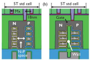
New materials, new transistor structures, new integration schemes: many of the boost scaling options being investigated by research teams around the world will be represented at the 2021 Symposia on VLSI Technology & Circuits – running as a virtual event from June 13 to 19. Just as a teaser, in this article we will briefly summarize a handful of papers from the Technology program, to give a taste of some current research trends. Benefits of forksheet over nanosheet One of the papers presented by Belgian research institute Imec is meant to demonstrate the benefits of forksheet transistors over nanosheet transistors for CMOS area scaling. Forksheet devices are lateral nanosheet devices with a forked gate structure. The physical separation of N- and PFETs by a dielectric wall enables N-P space scaling and consequently sheet width maximization – compared to a N-P nanosheet configuration – for the same footprint. According to Imec, forksheet transistors offer additional benefits in the manufacturing process. Firstly, for nanosheets the high mask aspect ratio is challenging for patterning a well-defined N-P boundary over the full stack height. Secondly, the pWFM (Work Function Metal) lateral etch in-between NMOS nanosheets can lead to mask undercut and therefore pWFM removal from PFETs. For forksheet devices, the mask aspect ratio at the N-P boundary is substantially lower because the mask edge lands on top of the wall. In addition, the risk of pWFM removal from PFETs due to mask undercut is eliminated by the physical separation of the pWFM on either side of the wall, including along the gate trench side walls. Electrostatic control for forksheets and nanosheets is comparable. Read the rest of Moore’s Law extension a key theme at the 2021 VLSI Symposia Higher density DRAM alternative; faster simulations; new chip prototyping programMay 27th, 2021 by Roberto Frazzoli
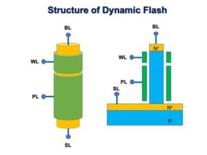
Chip shortage and foundry activity continue to make headlines. Tesla is reportedly considering paying in advance for chips to secure its supply, and is said to be even exploring the acquisition of a semiconductor fab. GlobalFoundries is reportedly working with Morgan Stanley on an initial public offering that could value the foundry at about $30 billion. Let’s now move to some process technology and EDA updates. Vertical nanowire-based memory promises 4X DRAM density without special materials Singapore-based Unisantis unveiled the developments of its Dynamic Flash Memory (DFM) technology at the recent IEEE International Memory Workshop. According to the company, DFM offers faster speeds and higher density when compared to DRAM or other types of volatile memory. DFM is also a type of volatile memory, but since it does not rely on capacitors it has fewer leak paths, and it has no connection between switching transistors and a capacitor. The result is a cell design with the potential for significant increases in transistor density. Additionally – as it offers ‘block erase’ like a Flash memory – DFM reduces the frequency and the overhead of the refresh cycle and can deliver significant improvements in speed and power compared to DRAM. Based on TCAD simulation, Unisantis claims that DFM can potentially achieve a 4X density increase compared to DRAM. So, while the scaling of DRAM has almost stopped at 16Gb, DFM could be used to build 64Gb memory devices. Unisantis points out that unlike the so-called ‘emerging memory technologies’ (MRAM, ReRAM, FRAM, PCM), its Dynamic Flash Memory does not require using additional materials on top of a standard CMOS process. DFM was developed by Unisantis with the principles of its patented surround gate transistor (SGT) technology, also referred to in the semiconductor industry as a vertical nanowire transistor. According to the company, the benefits of this technology include improved area density, compared to planar and FinFET transistors; reduced leakage power, due to the strong electrostatic control of the surrounding gate to the transistor channel; and the possibility of optimizing the transistor width and length for different power/performance combinations. Unisantis is working on SGT technology in collaboration with Belgian research institute Imec. Read the rest of Higher density DRAM alternative; faster simulations; new chip prototyping program Chip lead times; Samsung EUV lines in Austin; Google 3D videoconferencing; data-driven algorithm designMay 20th, 2021 by Roberto Frazzoli
Chip shortage and new fab plans continue to be hot topics this week, while there is no shortage of AI news – with Google announcing the next generation of TPUs, and Edge Impulse expressing an interesting concept about machine learning bound to replace code writing in algorithm design. Chip lead times reach 17 weeks According to a research by Susquehanna Financial Group, quoted by Bloomberg, chip lead times – the gap between order and delivery – increased to 17 weeks in April. That is the longest wait since the firm began tracking the data in 2017. Specific product categories reported even longer lead times: 23.7 weeks in April for power management chips, about four weeks more than a month earlier; industrial microcontrollers also showed a worsened situation, with order lead times extended by three weeks. Automotive chip supply continues to be a pain point, with NXP reportedly having lead times of more than 22 weeks now – up from around 12 weeks late last year – and STMicroelectronics to more than 28 weeks. This situation is raising concerns of ‘panic ordering’ that may lead to market distortions in the future. IBM’s 2nm chip; EDA updates; AI updates; acquisitionsMay 13th, 2021 by Roberto Frazzoli
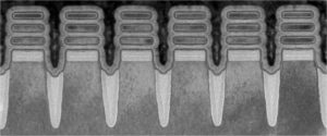
Catching up on some of the news from the last four weeks or so, the IBM 2-nanometer announcement definitely stands out as a major update. Several recent news also concerns EDA, as well as AI accelerators. Two of the newest updates about AI startups will translate into an additional $150 million pumped into this industry by investors. IBM’s 2-nanometer chip As widely reported by many media outlets, last May 6 IBM announced the development of the world’s first chip with 2-nanometer nanosheet technology. The result was achieved by IBM research lab located at the Albany Nanotech Complex in Albany, NY, where IBM scientists work in collaboration with public and private sector partners. According to the company, IBM’s new 2-nanometer chip technology will achieve 45 percent higher performance, or 75 percent lower energy use, than today’s most advanced 7-nanometer node chips. Reporting about the announcement, EETimes underlined that this chip is the first to use extreme-ultraviolet lithography (EUV) for front-end of line (FEOL) processes. Other details reported by EETimes include the use of bottom dielectric isolation to eliminates leakage current between nanosheets and the bulk wafer; and a novel multi-threshold-voltage scheme. Reportedly, IBM expects 2-nanometer foundry technology based on this work to go into production towards the end of 2024. Read the rest of IBM’s 2nm chip; EDA updates; AI updates; acquisitions A closer look at Cadence’s new Palladium Z2 Enterprise Emulation and Protium X2 Enterprise Prototyping systemsMay 7th, 2021 by Roberto Frazzoli
As gate count of advanced chips gets bigger and bigger, design teams need more powerful emulation and prototyping systems to reduce time-to-market. Cadence, for its part, is responding to this need with the introduction of its Palladium Z2 Enterprise Emulation and Protium X2 Enterprise Prototyping systems, the latest generation of a coordinated solution that the company has dubbed “Dynamic Duo”. Let’s now take a closer look at these two new systems with the help of Paul Cunningham, Senior Vice President, System & Verification Group at Cadence, who recently gave a video interview on this topic to Sanjay Gangal from EDACafe.
EDACafe interviews Paul Cunningham, Senior Vice President, System & Verification Group at Cadence Doubled capacity, 50% performance increase The key to improved performance and capacity – compared to the previous generation of these systems, Palladium Z1 and Protium X1 – is the adoption of new processing engines. “They are powered by two different chips,” Cunningham explained. “Palladium Z2 is powered by a custom ASIC we actually built here at Cadence, (…) and Protium X2 is based on a massive capacity, leading edge Xilinx FPGA, the VU19P.” As Cunningham pointed out, Cadence has built two entirely new platforms around these chips, with new rack and new boards, achieving significant results: “Within the same rack footprint [as the previous generation], we are doubling the capacity per rack and we are increasing the performance by 50%. So there’s a very significant uplift in both these platforms.” New AI architectures in the spotlight at Linley Spring Processor Conference 2021April 29th, 2021 by Roberto Frazzoli
Cerebras’ new 2.6 trillion transistors wafer scale chip is one the announcements made during the 2021 edition of the Linley Spring Processor Conference, a virtual event organized by technology analysis firm The Linley Group from April 19 to 23. In our quick overview of the conference we will focus mainly on new product announcements, which include innovative AI intellectual property from startups Expedera and EdgeCortix, a new approach to clock distribution from Movellus, and more. But first, let’s briefly summarize the opening keynote given by Linley Gwennap – Principal Analyst of The Linley Group – who provided an updated overview of AI technology and market trends. A variety of AI acceleration architectures Gwennap described the different AI processing architectures that the industry has developed over the past few years. While many CPUs, GPUs, and DSPs include wide vector (SIMD) compute units, many AI accelerators use systolic arrays to break the register-file bottleneck. Also, convolution architecture optimized for CNNs have been proposed: examples include processors developed by Alibaba and Kneron. Within AI-specialized architectures, many choices are possible: a processor can use many little cores, or a few big cores. Extreme examples are Cerebras with its wafer-scale chip integrating over 400,000 cores (850,000 in the latest version), and Groq with one mega-core only. Little cores are easier to design, while big cores simplify compiler/software design and are better for real-time workloads. Another architectural choice is between multicore versus dataflow: in a multicore design, each core executes the neural network from start to finish, while in a dataflow design the neural network is divided across many cores. An additional architectural style – that goes ‘beyond cores’ – is Coarse-Grain Reconfigurable Architecture (CGRA), which uses dataflow principles, but instead of cores, the connected blocks contain pipelined compute and memory units. This approach has been adopted by SambaNova, SimpleMachines, Tsing Micro and others. So the industry now offers a wide range of AI-capable architectures, ranging from very generic to very specialized. In general terms, a higher degree of specialization translates into higher efficiency but lower flexibility. Read the rest of New AI architectures in the spotlight at Linley Spring Processor Conference 2021 EDA startup Avishtech innovates PCB stack simulation and loss modeling of PCB transmission linesApril 22nd, 2021 by Roberto Frazzoli
Selecting the right construction for a PCB stack and meeting the tight loss budget of PCB transmission lines are major challenges for designers and manufacturers of high-frequency printed circuit boards. According to Avishtech – a young San Jose-based provider of innovative EDA solutions – traditional EDA tools fall short of needs in those two areas, often leading to a trial-and-error development process that translates into long design cycles and increased costs. Avishtech started addressing these problems in 2019. “That’s when me and my partners saw an opportunity to really make an impact and actually do things in a very different way,”, said founder and CEO Keshav Amla in the video interview he recently gave to Sanjay Gangal from EDACafe. “We had the right backgrounds and we felt that we were the right people to do that.” So after completing his master’s degree, in 2019 Amla left his PhD program to work on Avishtech full-time. One year later, in July 2020, the company launched its Gauss product line: Gauss Stack, a PCB stack-up design and simulation solution, and Gauss 2D, a field solver that improves transmission line loss modeling. Let’s now take a closer look at Avishtech and at the recently announced latest versions of its tools.
Nvidia’s datacenter CPU; fast AI training on x86; Siemens acquires OneSpin; EDA Q4 resultsApril 15th, 2021 by Roberto Frazzoli
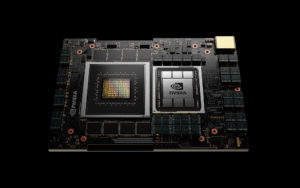
Nvidia entering the datacenter CPU market – and becoming a direct competitor of Intel in this area – is definitely this week’s top news. Unrelated to this announcement, an academic research adds to the debate on heterogeneous compute. More updates this week include an important EDA acquisition and EDA figures; but first, let’s meet Grace. Grace, the new Arm-based Nvidia datacenter CPU Intel’s recently appointed CEO Pat Gelsinger is facing an additional challenge: defending the company’s datacenter CPU market share against Grace, the new Nvidia CPU – that promises 10x the performance of today’s fastest servers on the most complex AI and high performance computing workloads. Announced at the current GTC event and available in the beginning of 2023, the new Arm-based processor is named for Grace Hopper, the U.S. computer-programming pioneer. In his GTC keynote, Nvidia CEO’s Jensen Huang explained that Grace is meant to address the bottleneck that still makes it difficult to process large amounts of data, particularly for AI models. His example was based on half of a DGX system: “Each Ampere GPU is connected to 80GB of super-fast memory running at 2 TB/sec,” he said. “Together, the four Amperes process 320 GB at 8 Terabytes per second. Contrast that with CPU memory, which is 1TB large, but only 0.2 Terabytes per second. The CPU memory is three times larger but forty times slower than the GPU. We would love to utilize the full 1,320 GB of memory in this node to train AI models. So, why not something like this? Make faster CPU memories, connect four channels to the CPU, a dedicated channel to feed each GPU. Even if a package can be made, PCIe is now the bottleneck. We can surely use NVLink. NVLink is fast enough. But no x86 CPU has NVLink, not to mention four NVLinks.” Huang pointed out that Grace is Arm-based and purpose-built for accelerated computing applications of large amounts of data – such as AI. “The Arm core in Grace is a next generation off-the-shelf IP for servers,” he said. “Each CPU will deliver over 300 SPECint with a total of over 2,400 SPECint_rate CPU performance for an 8-GPU DGX. For comparison, todays DGX, the highest performance computer in the world, is 450 SPECint_rate.” He continued, “This powerful, Arm-based CPU gives us the third foundational technology for computing, and the ability to rearchitect every aspect of the data center for AI. (…) Our data center roadmap is now a rhythm consisting of three chips: CPU, GPU, and DPU. Each chip architecture has a two-year rhythm with likely a kicker in between. One year will focus on x86 platforms, one year will focus on Arm platforms. Every year will see new exciting products from us. The Nvidia architecture and platforms will support x86 and Arm – whatever customers and markets prefer,” Huang said. The NVLink interconnect technology provides a 900 GB/s connection between Grace and Nvidia GPUs. Grace will also utilize an LPDDR5x memory subsystem. The new architecture provides unified cache coherence with a single memory address space, combining system and HBM GPU memory. The Swiss National Supercomputing Centre (CSCS) and the U.S. Department of Energy’s Los Alamos National Laboratory are the first to announce plans to build Grace-powered supercomputers. According to Huang, the CSCS supercomputer, called Alps, “will be 20 exaflops for AI, 10 times faster than the world’s fastest supercomputer today.”. The system will be built by HPE and come on-line in 2023. |
|
|
|||||
|
|
|||||
|
|||||


