


EDACafe Editorial Roberto Frazzoli
Roberto Frazzoli is a contributing editor to EDACafe. His interests as a technology journalist focus on the semiconductor ecosystem in all its aspects. Roberto started covering electronics in 1987. His weekly contribution to EDACafe started in early 2019. Samsung Foundry’s roadmap; AI EDA startups; 100x CPU performance boost; new ECC methodJune 20th, 2024 by Roberto Frazzoli
Not surprisingly, Samsung Foundry’s recent event confirmed at least two of the trends also recently highlighted by TSMC: the adoption of backside power delivery and the development of technologies that make it possible to place an electric chip and an optical chip in the same package. A frivolous remark on process naming: contrary to Intel Foundry and TSMC, Samsung has not switched to the Angstrom unit and prefers using tenths of a nanometer, with a point (SF1.4). Probably the most surprising announcement this week comes from a Finnish startup, claiming that it can boosts the performance of any existing multicore CPU up to 100-fold. An obvious question comes to mind: why haven’t the leading CPU vendors of the world come up with a similar solution yet? We’ll try to find out as soon as we can. Roadmap updates from the U.S. Samsung Foundry Forum At the recent U.S. Samsung Foundry Forum, the South Korean company announced two new process nodes, SF2Z and SF4U. The company’s latest 2-nanometer process, SF2Z, incorporates optimized backside power delivery network (BSPDN) technology, enhancing PPA compared to SF2 and reducing voltage drop. Mass production of SF2Z is slated for 2027. SF4U is described as a “high-value” 4-nanometer variant that offers PPA improvements by incorporating optical shrink, with mass production scheduled for 2025. Samsung also reaffirmed that its preparations for SF1.4 (1.4-nanometer) are progressing smoothly, with performance and yield targets on track for mass production in 2027. The company emphasized the maturity of its GAA (gate-all-around) technology, which will be used to mass produce Samsung’s second-generation 3-nanometer process (SF3) in the second half of this year and the upcoming 2-nanometer process. Another highlight was the unveiling of Samsung AI Solutions, a turnkey AI platform resulting from collaborative efforts across the company’s Foundry, Memory and Advanced Package businesses, enabling a 20% improvement in total turnaround time. The company is also planning to introduce integrated, co-packaged optics (CPO) technology. 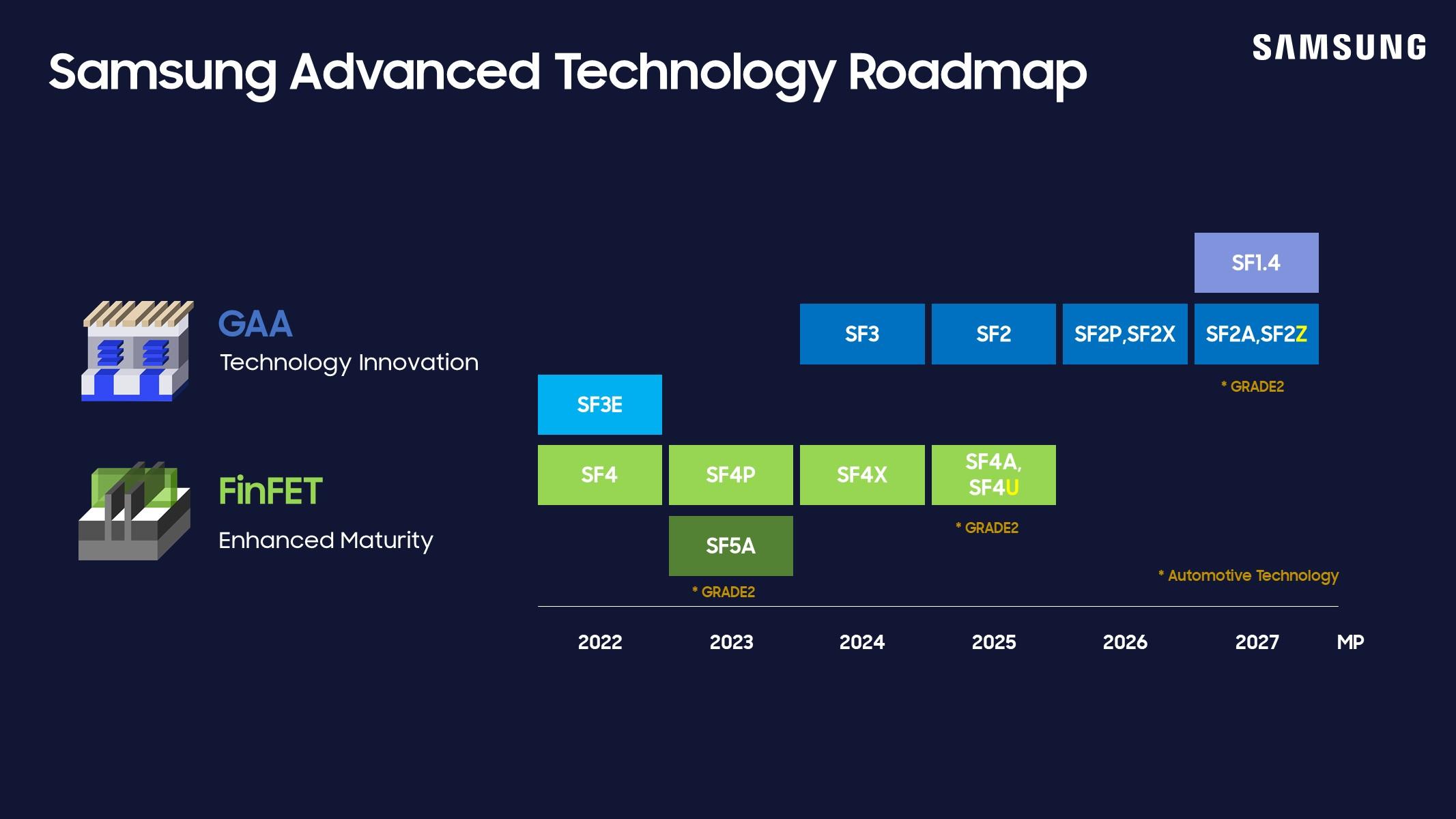 Credit: Samsung Foundry
As usual, on occasion of the event, the “big three” EDA vendors announced the certification of their tools for the latest Samsung Foundry processes. Here is just a short hint to their announcements, with links to their respective, detailed press releases. Cadence has announced a broad collaboration with Samsung Foundry that includes technology advancements to accelerate design for AI and 3D-IC semiconductors, including on Samsung Foundry’s most advanced GAA nodes. Among other things, Siemens and Samsung Foundry recently collaborated to update process design kits that integrate into Siemens’ Xpedition Substrate Integrator (XSI) software and Xpedition Package Designer (XPD) software. Synopsys has announced that its AI-driven digital design and analog design flows have achieved certification on Samsung Foundry’s SF2 process with multiple test chip tapeouts. The Samsung SF2 process was optimized using Synopsys’ AI-driven design technology co-optimization (DTCO) solution. The same co-optimization techniques will be applied for Samsung’s SF1.4 process. AI EDA startups at DAC EDA startups still exist, and – not surprisingly – some of them are leveraging AI technologies. Verific’s booth at DAC will host two EDA startups: Primis.ai offers a generative AI solution for chip design with language-to-code and language-to-verification capabilities; Silimate is building the co-pilot for chip designers to help build better chips faster. A third Verific startup customer, Metalware, accelerates embedded development using AI technology. On-die voltage regulation solutions from Movellus Movellus has introduced the Aeonic Power product family aimed at meeting the on-die power delivery needs of computational blocks, functional blocks, and die-to-die interconnects for complex SoCs. The family currently includes two products: Aeonic Power HC, enabling energy optimization of digital cores and logic blocks, and Aeonic Power LN to simplify power delivery for die-to-die interfaces (e.g. UCIe). According to Movellus, on-die voltage regulation holds tremendous potential to reduce power, simplify design, and increase the robustness of power delivery networks, but to date, only a handful of companies had the capability to tackle this using custom designs. Aeonic Power aims to make these solutions available to the broader market. Finnish startup promises 100x CPU performance improvement Finland-based Flow Computing has emerged from stealth announcing four million Euro pre-seed funding from several Nordic VC’s and business entities. Flow is proposing a new architecture, referred to as a Parallel Processing Unit (PPU), claiming that it can boosts the CPU performance up to 100-fold. The PPU is capable of being integrated on-die into any CPU design architecture, through a license from Flow, and is fully backwards compatible with every existing software application for that CPU architecture. According to Flow, the PPU even eliminates the need for expensive GPU acceleration of CPU instructions in performant applications. Some technology details can be found here. In short, Flow achieves this result by combining three innovations that address the limitations of current multicore CPUs: 1) Using latency time to do something. Latency of memory references is hidden by executing other threads while accessing the memory. 2) Reducing waste of time in synchronization of threads. Synchronizations are needed only once per step since the threads are independent of each other within a step and are overlapped with the execution. 3) Better handling of low-level parallelism. Functional units are organized as a chain where a unit can use the results of its predecessors as operands. Pipeline hazards are eliminated. New DRAM Error Correction Coding technology from ScaleFlux ScaleFlux has come up with a new ECC (Error Correction Coding) technology based on “list decoding”, claiming better correction performance for DRAM errors than conventional methods. The company has also engineered a highly parallel “VLSI-friendly” architecture for ultra-low-latency decoding. According to ScaleFlux, the new ECC technology accommodates less reliable, lower-cost DRAM chips, thus reducing the total cost of ownership for data center operators. A RISC security alliance Six founding members have established the CHERI Alliance to advance the industry-wide adoption of the security technology CHERI (Capability Hardware Enhanced RISC Instructions). The initial founding members include Capabilities Limited, Codasip, the FreeBSD Foundation, lowRISC, SCI Semiconductor, and the University of Cambridge. CHERI is a hardware-based technology developed by the University of Cambridge to fight cyber attacks that take advantage of memory issues. End-to-end PCIe optical connectivity from Astera Labs Astera Labs has unveiled what it claims is the industry’s first demonstration of end-to-end PCIe optical connectivity to provide unprecedented reach for larger, disaggregated GPU clusters. The company’s technology for PCIe over optics enables the use of PCIe and CXL connectivity even in row-to-row topologies throughout the data center, up to a distance of fifty meters or more. Mergers and acquisitions South Korea’s AI chip developers Rebellions and Sapeon have reportedly agreed to merge. The new entity is expected to be established in the third quarter of this year. Rebellions will be responsible for the management of the new entity, which will likely be led by Rebellions’ CEO. Sapeon is a subsidiary of SK Telecom. EDA vendor Primarius has acquired Belgium-headquartered Magwel, a provider of 3D solver- and simulation-based layout analysis and design solutions for digital, analog/mixed-signal, power and RF ICs. Magwel’s chip-level HBM ESD analysis platform, its power device design and layout verification tool suite and other technologies are now integrated into the Primarius portfolio. Further reading SemiAnalysis dives into the challenges of building GPU clusters with over 100,000 GPUs, the next step in the race towards training the next generation of AI models. A 100,000 GPU cluster will require more than 150 megawatt in datacenter capacity and use 1.59 terawatt hours in a single year, but power isn’t the only challenge. More problems to be solved concern datacenter networking and reliability. |
|
|
|||||
|
|
|||||
|
|||||


 Animation, 3D Art and 3D Models")