


EDACafe Editorial Roberto Frazzoli
Roberto Frazzoli is a contributing editor to EDACafe. His interests as a technology journalist focus on the semiconductor ecosystem in all its aspects. Roberto started covering electronics in 1987. His weekly contribution to EDACafe started in early 2019. Special report: DAC and Semicon West 2023July 19th, 2023 by Roberto Frazzoli
Artificial intelligence, Moore’s law, chiplets, and High NA EUV were among the themes discussed by keynoters and panelists at the two industry events, both held in San Francisco from July 9-10 to July 13 Thousands of industry professionals and academic researchers involved in all different aspects of the semiconductor ecosystem gathered in San Francisco last week – either as attendees, exhibitors, presenters, or speakers – for the 2023 editions of the Design Automation Conference and Semicon West. Back to normal after the pandemic, the two co-located events offered a rich menu to the semiconductor community – combining research papers, exhibition floors, keynotes and panels. Adding to this offering, Semicon West was also co-located with the Flex event, and two European semiconductor research institutes – Belgium’s imec and France’s CEA-Leti – also organized their own forums at venues nearby (ITF Semicon USA and Leti Semicon Workshop, respectively). Here we will try to summarize some of the concepts that emerged from some of the keynotes and panels. EDA: no disruptions ahead Let’s start with EDA. Overall, it looks like the industry is not expecting any major disruptions on the short term. Artificial intelligence will obviously continue to play a key role in the evolution of EDA tools, but today this can be taken for granted and cannot be considered a new trend anymore. Part of the debate about EDA concerned the adaptation of existing EDA tools to the change of external conditions, such as the advent of cloud computing. The lack of disruptive innovations was effectively summarized by a rather provocative questions asked by Prit Banerjee, Ansys’ CTO, to EDA veterans Joe Costello and Wally Rhines during a panel. In short, Banerjee – speaking from the audience, not as a panelist – maintained that until now the major EDA vendors have just “tweaked” their EDA tools to adapt them to new technologies – such as parallel processing, AI, cloud computing – and asked if there is now space for a new EDA flow that is natively optimized for those new resources. Joe Costello answered that it’s a great idea, but today it would be difficult to find the money to undertake such an effort.
An example of the adaptation of EDA tools to new resources concerns cloud computing. A DAC panel addressed this theme, and most panelists agreed on saying that cloud-based EDA solutions are not fully optimized yet. Among the missing elements are a specific methodology guiding EDA users to take advantage of cloud resources; cloud-native algorithms; and the ability to keep up with innovations in cloud services. Also in terms of EDA evolution, Berkeley professor and EDA veteran Alberto Sangiovanni-Vincentelli in his keynote emphasized the need for new methodologies for the design of ‘cyberphysical systems’ – in other words, products combining a mechanical part and semiconductors, such as cars. Mechanics requires different equations from electronics, and currently there are no solutions to describe mechanical systems at a high abstraction level. Equations vs artificial intelligence Artificial intelligence was a major topic at this DAC, not just in terms of its role in EDA but also through a conference track dedicated to AI algorithms and other specific program items. But AI continues to be a controversial issue – or, at least, an authoritative scientist keeps warning about its dangers and limitations. In his keynote and in a panel, Alberto Sangiovanni-Vincentelli reiterated his view: scientist should try to explain things by writing equations in the first place, instead of resorting to artificial intelligence. AI systems such as ChatGPT are “stupid”, he said, because they are based on a brute force approach (scanning enormous amounts of data), and tapping into the Internet as a source to answer questions they sometimes rely on fake information. “Garbage in, garbage out”, he said. The brute force approach is also the reason why AI bias – racial bias, for example – is difficult to eradicate, since it’s impossible to find its root cause among billions of parameters. Sangiovanni-Vincentelli therefore suggested to combine AI with proven physics knowledge, using the former as a tool to reduce the search space. This, he said, is how DeepMind managed to successfully create an AI program – AlphaFold2 – that predicts the 3D structure of a protein using its amino acid sequence as an input. By merging AI with physics knowledge, AI can continue to play a role in the future evolution of EDA; as opposed to previous AI waves – such as expert systems in the 80s – whose EDA applications did not survive. 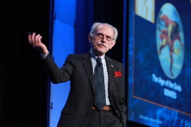 Alberto Sangiovanni-Vincentelli. Source: DAC Facebook page AI in EDA: will Fully Homomorphic Encryption take it to the next level? As for the role being played by artificial intelligence in EDA, a panel devoted to this theme revealed a general agreement on the need for benchmarks and for more design data to train AI models – but chip design companies are not willing to share their design data. EDA veteran Wally Rhines – in his keynote – elaborated on this issue. He said that the data that is needed to enable EDA to proceed to the next level – “generative design”, design generated from requirements – includes the whole “design journey” of different versions, including the ones that were scrapped. He then proposed to address the data secrecy issue using Fully Homomorphic Encryption, which would enable chip design companies to share their design data without making them public. FHE, as it is known, allows encrypted data to be processed without prior decryption – and Rhines is currently the CEO of Cornami, a startup that develops special processors for FHE. Rhines admitted that FHE requires a large amount of processing power – provided by processors with an extremely long word, such as 10,000 bits – and produces big volumes of data. According to Rhines, FHE will be commercially available in two years, and then “the world changes”. DARPA is also working on FHE with its Dprive program.  Wally Rhines. Source: DAC Facebook page Moore’s law: alive for the next ten years, or dead ten years ago? As for Semicon West, a key message from many speakers was that Moore’s law is alive: the industry is already developing technological solutions that will enable further shrinking of the transistor size, over several new process nodes spanning the next decade or so. There seems to be a general agreement on a roadmap which – after GAA – will move to the Complementary FET architecture, with vertically stacked transistors. According to Luc Van den hove, imec’s President and CEO, lithography scaling must continue because it provides an exponential complexity increase, whereas 3D stacking can only provide a linear complexity increase. However, 3D solutions such as wafer stacking will be needed to address the so called ‘memory wall’: according to Van den hove, in certain AI-HPC applications the processor only works 3% of its time, spending the remaining 97% waiting for data. A dissonant voice came from DAC. In his keynote, Mark Horowitz from Stanford University said that Moore’s law is dead and that chiplets are not a solution. According to Horowitz, the meaning of Moore’s law always gets misunderstood as it actually refers to transistor cost – not to transistor size as such. And in terms of cost, the benefits of scaling have ended years ago – as transistors built with the most advanced process nodes are more expensive, not cheaper. Chiplets are not going to change this; the cost of silicon per area unit will still depend on the process node, and in addition to that some expensive packaging will be needed. Nonetheless, everyone still assumes that the available processing power will continue to grow at the same pace it did over the last decades, with no additional price. Ever more complex algorithms continue to be encouraged because of this – and Fully Homomorphic Encryption comes to mind after this observation. Horowitz therefore envisions a complete paradigm change, where application designers (software programmers involved in the development of end products) will be able to create their own chips by adding predesigned hardware modules to a platform, in a way similar to downloading a smartphone app from an app store. Changing the current chip design market is impossible, he said; instead of helping existing chip designers, what should be done is to create a new market, serving a new category of users.  Mark Horowitz. Source: DAC Facebook page So, is Moore’s law dead or alive? Transistor size reduction will undoubtedly continue, as the technology to do that is already being developed (see next paragraph). As for transistor cost, a reduction seems to be unlikely, given the extreme complexity of the future technologies. Cost, however, depends on many factors – including economies of scale – and is therefore difficult to predict on the long term. New challenges posed by High NA EUV lithography Lithography scaling was also the subject of a day-long series of presentations (a TechTalk) at Semicon West, where the main theme was the future advent of high numerical aperture EUV lithography equipment. According to imec, High NA EUV will be introduced around the A14 process node. High NA EUV will undoubtedly enable further transistor scaling, but it will also involve a number of new problems as – on certain aspects – its performance will be lower than current EUV equipment. For example, shorter depth of field will require better focus accuracy, which will mean thinner resist and the need for better wafer planarity and better metrology (one order of magnitude more accurate). And a smaller projection area will mean smaller reticle size, in sharp contrast with the current trend towards bigger chips. However, solutions to overcome these problems are already being developed: some of them were described during this presentation by Tokio Electron, IBM, LAM (which is proposing the use of dry resist) and more. As for the smaller reticle size, this limitation does not necessarily sound like a big problem assuming that the industry is moving towards chiplets which are small by definition. As for patterning, a DAC panel advocated the transition from Manhattan shapes (rectangles) to curvy design. Panelists maintained that curvy design provides many benefits – in terms of yield, wire length reduction, mask variability, DRC violations etc. – and that it can be adopted today without totally rewriting all EDA tools. Masks with curvy shapes can be written using a multibeam writer. The chiplet trend Except for Mark Horowitz, there seems to be a general agreement on the future role of chiplets as a way to extend Moore’s law. Alberto Sangiovanni-Vincentelli, for his part, praised the benefits of this approach – among them, shorter connections – quoting the AMD Zen architecture and Marvell’s MoChi attempt to create a range of standard chiplets. Luc Van den hove from imec cited the flexibility benefit of chiplets in application such as automotive, where a large number of ECU variants will be produced in smaller volumes due to the slow growth of the car market. Contributions to an history of EDA Mark Horowitz’s keynote was also interesting from the point of view of the history of EDA, as he used the birth of EDA as an example of creation of a new market to serve a new category of users. According to Horowitz, EDA tools were initially created to enable logic designers to design chips, even though they knew nothing about transistors. In those early days, “real” chip designers – experts in managing aspects such as wire length effects etc. – did not want to use automatic placement and routing tools. It’s an interesting perspective, as the term “automation” tends to emphasize the designer productivity aspect, whereas in Horowitz’s view the key point seems to be decoupling logic design from silicon physics as much as possible. As for the entrepreneurial aspect of EDA history, a contribution came from an already mentioned panel when Wally Rhines credited Joe Costello of having been the first tech CEO to start acquiring smaller companies as a growth strategy. An extensive transcript of this panel has been provided by Semiconductor Engineering. Chips Acts vs free trade Geopolitical issues did not get much space from keynoters and panelists at either DAC or Semicon West. Some of the speakers who did touch on these themes, however, appeared to disagree with the underlying goal of most Chips Acts around the world, gaining independence from other countries. Speaking to a mostly US audience, Luc Van den hove from Belgium-based imec said – not surprisingly – that individual countries should not try to do everything by themselves when it comes to their semiconductor ecosystem. They should avoid duplication of efforts and avoid decoupling from other areas of the world. Joe Costello, at two different panels, ironized about Trump waking up China’s government to the strategic importance of semiconductors, with the result of creating a potentially strong competitor. No co-location for the 2024 events DAC 2024 will take place in San Francisco from June 23 to 27; Semicon West will also return to San Francisco next year, but from July 9 to 11. |
|
|
|||||
|
|
|||||
|
|||||


 Animation, 3D Art and 3D Models")