


EDACafe Editorial Roberto Frazzoli
Roberto Frazzoli is a contributing editor to EDACafe. His interests as a technology journalist focus on the semiconductor ecosystem in all its aspects. Roberto started covering electronics in 1987. His weekly contribution to EDACafe started in early 2019. Japan’s 2-nm effort; die-to-die interfaces; MediaTek’s activity; 1.53 Pbit/s on fiber; FinFET-based acoustic resonatorsNovember 18th, 2022 by Roberto Frazzoli
Geopolitical tensions keep making headlines, with Japan trying to catch up on advanced nodes capabilities to gain more independence from foreign suppliers. Western world investments in new fabs continue, with Infineon planning for the construction of a factory for 300-millimeter analog/mixed-signal and power semiconductors in Dresden, Germany. More news this week include three interesting academic research works. Japanese government to subsidize a new domestic chipmaker As reported by The Japan Times, eight major Japanese companies have jointly invested to launch a new firm, named Rapidus, tasked with developing 2-nanometer chips by 2027, in collaboration with IBM. The eight companies – Toyota, Sony, NTT, SoftBank, Kioxia, Denso, NEC and MUFG Bank – invested a total of ¥7.3 billion ($52 million) to form the new venture, which is chaired by Tetsuro Higashi, former president of chip equipment firm Tokyo Electron. The Japanese government plans to provide the new company with ¥70 billion ($500 million) in subsidies, backed by a second extra budget. Japan will also create a new body for chip research and development called ‘Leading-edge Semiconductor Technology Center’ (LSTC) by the year’s end, consisting of Japan’s major research bodies and universities. Reportedly, analysts are skeptical about the success of Rapidus, as the financial support promised by the Japanese government so far is much smaller than the amounts set out by the U.S. and the European Union for their ‘chips acts’, $52.7 billion and €43 billion ($45 billion) respectively.
EDA updates: Real Intent, Altium Real Intent has announced SafeConnect, a user-defined connectivity & glitch static sign-off tool. SafeConnect enables early RTL and netlist sign-off within IP blocks or across SoCs. Design and verification engineers can define rules for various source-destination types. SafeConnect has low noise reporting and integrated debug. The product is deployed during RTL design and post-synthesis. According to Real Intent, SafeConnect is expected to be about ten times faster than formal solutions and Tcl-based scripting. Altium has recently licensed Keysight’s advanced electromagnetic simulation technology to develop power analysis solutions for PCB designers. Power Analyzer, the first product resulting from this partnership, provides interactive analysis of power integrity issues affecting the power plane – through analysis of voltage drop and current density – from within the PCB layout environment. The solution aims at avoiding prototype re-spins, even without resorting to power integrity specialists. Die-to-die interfaces on 5-nanometer: Fraunhofer, Eliyan German research institute Fraunhofer IIS/EAS has announced their first implementation of the Bunch of Wires (BoW) standard-based interface IP on Samsung’s 5-nanometer technology. The institute managed to implement a data rate of 16 Gbit/s per lane – the highest rate specified by the BoW standard. Fraunhofer’s goal with this work is to extend the benefits of chiplet technology to electronic products with small production runs. Eliyan (Santa Clara, CA) has announced the successful tapeout of its NuLink technology on an industry standard 5-nanometer process. NuLink technology, which is a superset of BoW and UCIe, uses a standard, organic chip substrate eliminating the need for advanced packaging solutions, such as silicon interposers that limit overall system-in-package size. A flurry of new products from MediaTek In a few days’ timeframe – from November 8 to 11 – Taiwan-headquartered MediaTek made four tech-packed announcements: Dimensity 9200, its latest 5G chipset, which integrates an Arm Cortex X3 with operating speeds over 3GHz and the Arm Immortalis-G715 GPU with a hardware-based ray tracing engine; new Kompanio chipsets for entry level Chromebooks; the Pentonic 1000, its latest flagship smart TV SoC designed for 4K 120Hz displays, supporting Wi-Fi 6/6E and allowing users to watch up to eight streams of content at once; the new T800 chipset solution for sub-6GHz and mmWave 5G networks, supporting download speeds of up to 7.9Gbps. Furthermore, Canadian reverse engineering firm TechInsights has discovered MediaTek’s first 5G mmWave chipset, the Dimensity 1050, in the Moto Edge 2022 (North America). TechInsights considers this a “disruptive event” as, until now, only top tier US devices were equipped with 5G mmWave capabilities. “Qualcomm and Samsung have previously enjoyed leadership positions in this market, but with the Dimensity 1050, MediaTek is becoming a noticeable contender by making 5G mmWave support more accessible to mid to low tier smart phone manufacturers.” 1.53 petabits per second on a 55-mode fiber Researchers from the Japanese ‘National Institute of Information and Communications Technology’ (NICT) in collaboration with Nokia Bell Labs, Prysmian Group, and the University of Queensland (Australia) succeeded in transmitting data at a rate of 1.53 petabits per second over 25.9 kilometers using 55 modes on a standard cladding diameter (0.125 mm) optical fiber. The 55 independent signal streams could be separated by 110 x 110 MIMO processing to recover the transmitted data. The system could successfully receive polarization multiplexed 16 QAM signals at 184 wavelengths in the C wavelength band, achieving a spectral efficiency of 332 bits/s/Hz. Further expansion can be expected by adopting multi-band wavelength-division multiplexing in the future. The expansion of fiber transmission capacity will enable the development of infrastructures for ‘Beyond 5G’ networks. 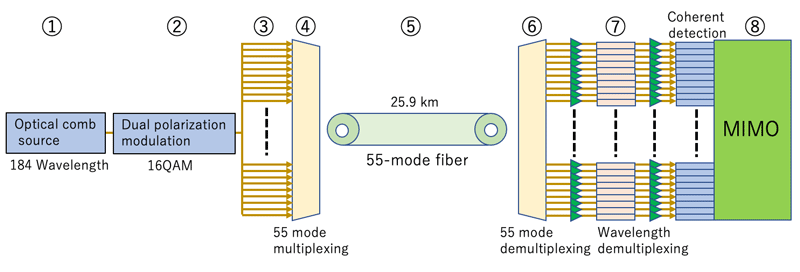 Credit: National Institute of Information and Communications Technology Real brain research suggests new types of neural networks The study of biological (real) brains suggests artificial intelligence advancements in terms of new neuron types and network topologies. Human Brain Project researchers from the Graz University of Technology (Austria) have trained a large-scale model of the primary visual cortex of the mouse, reproducing a number of the brain’s visual processing capabilities in a versatile and accurate way. In particular the capability to solve diverse visual processing tasks, also on temporally dispersed visual information, with remarkable robustness to noise. As detailed in the research paper, this model’s architecture and neurons markedly differ from those of deep neural networks used in current artificial intelligence. Acoustic resonators based on standard CMOS FinFETs A research team from Purdue University, Skyworks Solutions and Texas Instruments has developed a solution for fabricating acoustic resonators using FinFETs in a standard CMOS process. The devices use phononic waveguides for acoustic confinement and exploit metal–oxide–semiconductor capacitors and transistors to electromechanically drive and sense acoustic vibrations. The technology potentially enables the integration of acoustic resonators in CMOS chips without resorting to the addition of MEMS, that requires process customization. Acquisitions and mergers Germany-based Codasip, a provider of Risc-V processor IP and high-level processor design tools, has acquired UK-based Cerberus Security Labs, a specialist in cybersecurity for embedded systems. France-based Secure-IC, a provider of cybersecurity solutions for embedded systems and connected objects, has acquired the security business of Belgium-based Silex Insight. The move is mostly targeted at IoT applications. Lam Research has completed the acquisition of Semsysco, a provider of wet processing semiconductor equipment. With this addition, Lam gains capabilities in advanced packaging, including chiplet-based solutions. Lidar providers Ouster and Velodyne have entered into a definitive agreement to merge in an all-stock transaction. The companies aim to realize annualized cost savings of at least $75 million within nine months after closing the proposed merger. Further reading A blog post from Canadian reverse engineering firm TechInsights looks back at the history and evolution of TSMC’s process technologies, starting from 1987 with its 3-micron node, with several SEM images. |
|
|
|||||
|
|
|||||
|
|||||


 Animation, 3D Art and 3D Models")