


EDACafe Editorial Roberto Frazzoli
Roberto Frazzoli is a contributing editor to EDACafe. His interests as a technology journalist focus on the semiconductor ecosystem in all its aspects. Roberto started covering electronics in 1987. His weekly contribution to EDACafe started in early 2019. Cadence’s Certus, a new approach to speeding up full-chip optimization and signoffOctober 24th, 2022 by Roberto Frazzoli
Based on a parallel architecture and a ‘distributed optimization engine’, the new automated environment builds on Cadence’s implementation system (Innovus) and timing signoff solution (Tempus), and promises up to 10X faster closure for designs greater than ten million cells With SoCs targeted at advanced applications getting ever larger and complex, moving from block-level optimization to full-chip design closure has become a challenging and time-consuming task for design teams. The current, manual full-chip closure flow involves many steps and iterations – from assembly, static timing analysis, and optimization and signoff with hundreds of views. According to Cadence, today’s design teams often spend five to seven days per iteration to meet chip-level signoff timing and power requirements, therefore this error-prone process can take designers months to converge. Additionally, current methodologies are considered inefficient in terms of team collaboration and user experience. Addressing these problems, Cadence has recently launched Certus Closure Solution, an environment aimed at accelerating full-chip design closure by means of a parallel architecture and automation of previously manual tasks. Brandon Bautz – Senior Group Director of Product Management, responsible for the Cadence silicon signoff and verification product lines in the Digital & Signoff Group at Cadence – described the features of Certus in the video interview he recently gave to EDACafe’s Sanjay Gangal. In this article we will add some more details about Certus, building on that video interview and on the answers Bautz provided to our additional questions.
Pain point: moving from block-level optimization to chip-level closureAs Bautz pointed out, block-level optimization is already effectively addressed by existing EDA tools. “Cadence has always offered industry leading approaches to block level power-performance-area closure with Innovus and Tempus ECO. But in talking to customers and understanding their problems, we knew that the real challenge in design closure was moving to the full chip level. With block level, you don’t naturally have a large problem than you do at the full chip level. Large designs today are easily upward of over one billion placeable objects,” he continued. “And then naturally, with those large designs come advanced nodes, and that adds a whole new layer of complexity, especially related to signoff and signoff closure. The unpredictable characteristics of these advanced nodes make chip closure and chip schedules much more unpredictable. Similarly, with all these larger designs and advanced nodes come more aggressive product schedules. So obviously, our customers want to do bigger, faster, more complex designs in more compressed schedule. All these factors are working, frankly, against the designers, making their job much more difficult.” 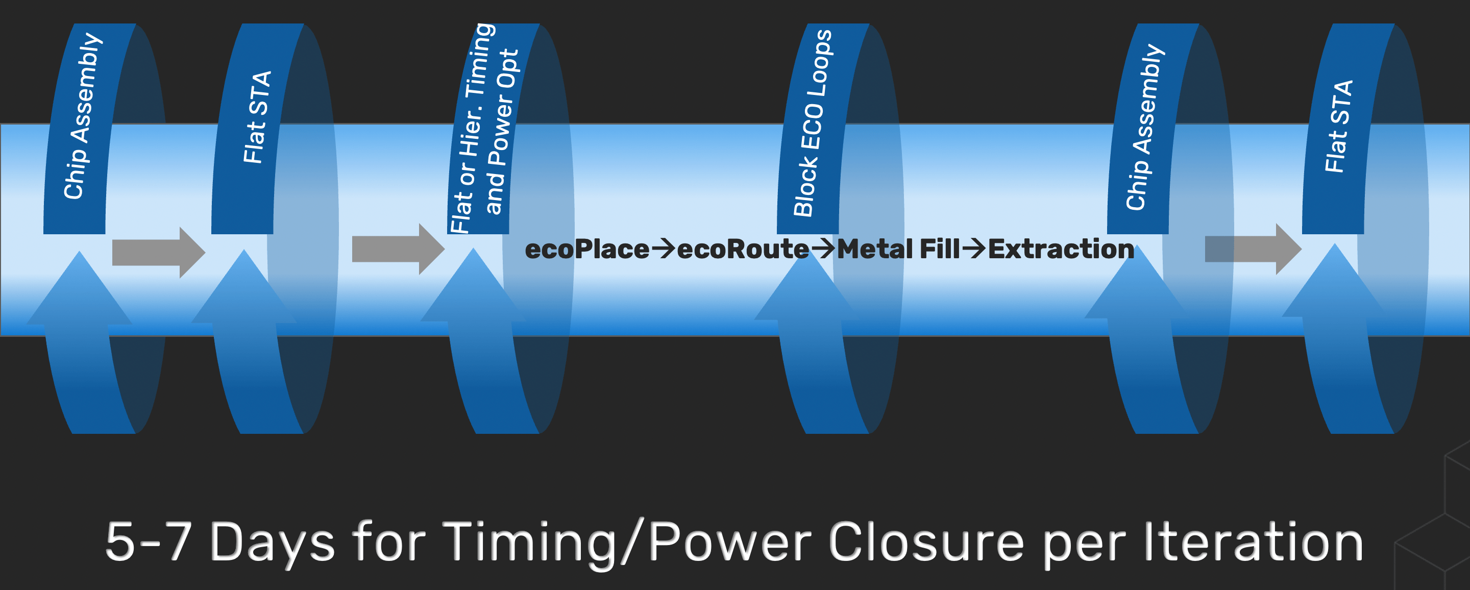 A visual representation of the manual full-chip closure flow, involving many iterations. Credit: Cadence A three-pronged approachTackling the challenges of full-chip signoff, Cadence has come up with a new environment based on a three-pronged approach: distributed processing, incrementality and automation. As Cadence explained, the new solution leverages the Concurrent Multi-Mode Multi-Corner (CMMMC) and Parallel Distributed Interactive MMMC (Paradime) technologies of the Tempus Timing Solution to deliver a fully automated flow and massively distributed for optimization and signoff. This allows concurrent, full-chip optimization through shared engines in the Innovus Implementation System and the Tempus Timing Solution. According to Cadence, the solution eliminates iterative loops with block owners and lets designers make quick optimization and signoff decisions. Furthermore, Certus uses the Tempus Timing Solution SmartMMMC Optimization capability to reduce the increasing number of signoff views. This way, Cadence claims, turnaround time and memory can be slashed by up to 4X. Running in parallel on multiple machinesAs Bautz pointed out, distributed processing is key to scalability: “We rewrote many of our optimization algorithms for distribution such that they can now run in parallel on multiple machines. And this has given the optimization engine and the timing engine the scalability needed to tackle full chip design closure. Partitioning is performed automatically by Certus following the design’s physical hierarchy.” As Cadence’s Paul McLellan noted in this blog post, “As is usual for a massively parallel system like this, there is a manager that controls what all the worker tasks do, and pulls the results together to decide what needs to be done next.” 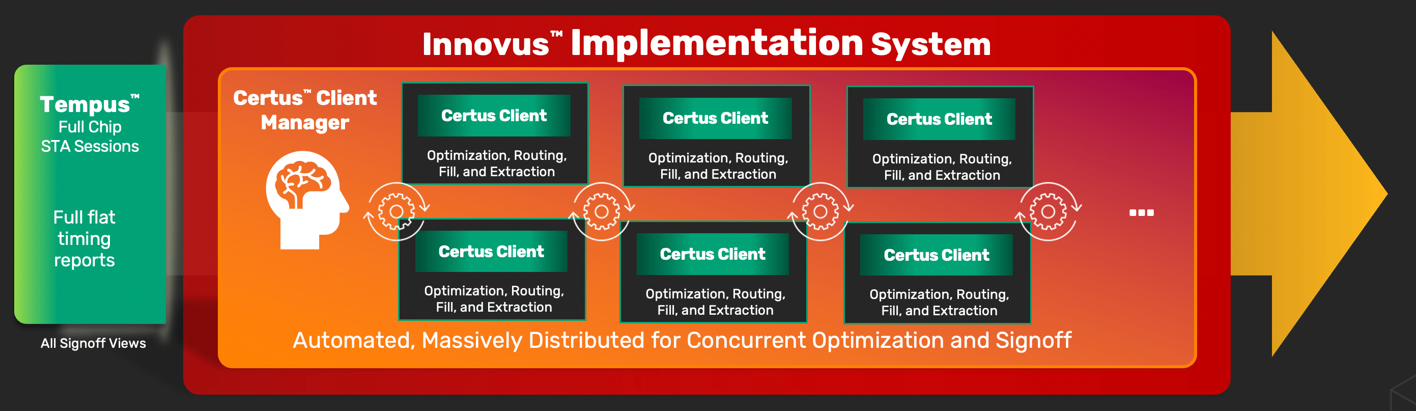 Credit: Cadence Incremental capabilitiesIn Certus, incremental signoff enables flexible restore and replacement of only the changed blocks. A second key differentiation is incrementality. When the optimization algorithm makes a change in the design, we want to be able to quickly see the impact of that change on the end result from a timing perspective. So we’ve introduced new incremental capabilities that make it much easier for the designer to load in just the block that changed, and then quickly see the net impact of that one block on the overall timing. Automation of the ECO cycleBautz also stressed another key capability of Certus: “The third [differentiation] is full automation. This really excites me as a former designer,” he said. “The typical ECO cycle today requires many engineers to run: of course to place and route, but also to incrementally run the place and route throughout the top level closure cycle.” (…) “The Certus environment – Bautz underlined – automates every step of the closure process, from chip-level timing analysis to block-level optimization (including reflecting changes within the different blocks) all the way through detailed routing, metal fill and parasitic re-extraction. Certus is launched by a single designer and driven from a single cockpit interface – this leads to the 10x productivity and empowered collaboration benefits.” Cadence describes the Certus interface as an enhanced interactive GUI that allows cross-probing for detailed timing debug. How Certus fits in the Cadence flowAs Cadence explained, Certus provides implementation in the Innovus Implementation System, metal fill with the Pegasus Physical Verification System, parasitic extraction with the Quantus Extraction Solution, and full static timing analysis with the Tempus Signoff Solution. Design teams can move from block-level to full-chip and sub-systems optimization and signoff closure with Tempus ECO, Tempus Timing Solution, and Cadence Certus—all without leaving the Innovus Implementation System environment. While, on the one hand, Certus manages the above-mentioned Cadence existing tools, it also executes its own unique code, such as its distributed optimization engine. “The distributed optimization engine is indeed a breakthrough and an excellent example of an algorithm re-architected for distributed execution,” Bautz commented. “[Certus] is truly integrated at the code level, so you’re not ping-ponging back and forth between different binaries. And that’s really how we can deliver first pass convergence at the full chip level, with the best power-performance-area possible,” he added. Certus is also integrated with the Cadence Integrity 3D-IC Solution, allowing users to close inter-die paths across heterogenous process dies. 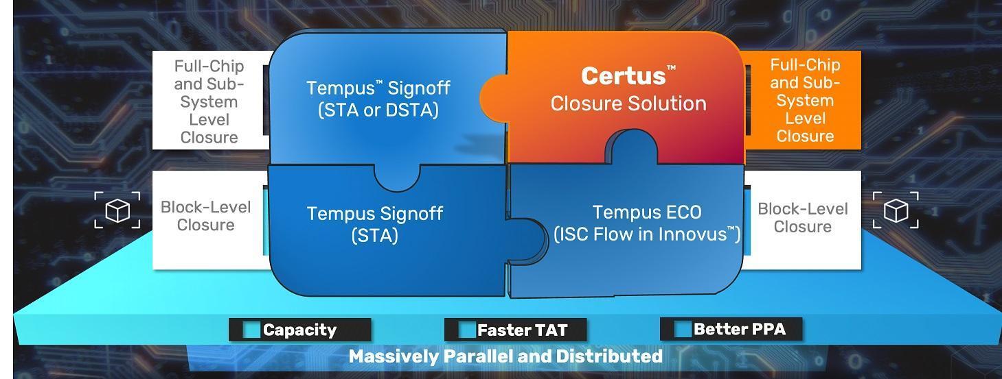 Credit: Cadence Design closure accelerationAccording to Cadence, Certus delivers ‘overnight turnaround time.’ “First and foremost, [Certus’ benefit] is absolutely productivity,” Bautz confirmed. “Going back to the schedule challenges, we knew we wanted to address headlong. So the automation coupled with that distributed optimization, greatly accelerates the wall times that one would experience there. Customers are seeing anywhere from three to 10X improvement in their overall turnaround time. This is what makes Certus highly scalable as design sizes grow, and ultimately leads to the productivity factor. Then, second [benefit is] capacity. With larger designs you have to have EDA tools and architectures that can scale to solve the problem. In the past, we’ve used a lot of different techniques, hierarchical methodologies and such to try to cope with large designs, but they have their inherent limitations and certain costs. With Certus, we can take the full flat timing and overlay that onto the hierarchical design so you get the most accurate slack and therefore the most predictable closure possible.” In the above-mentioned blog post, McLellan provided two Certus application examples. The first slide below concerns a design with 22 million instances in a 6-nanometer process, which ran in eleven hours achieving a 10X improvement. The second slide refers to a design with 140 million instances in a 16-nanometer process, which ran in thirteen hours achieving an 8X improvement. 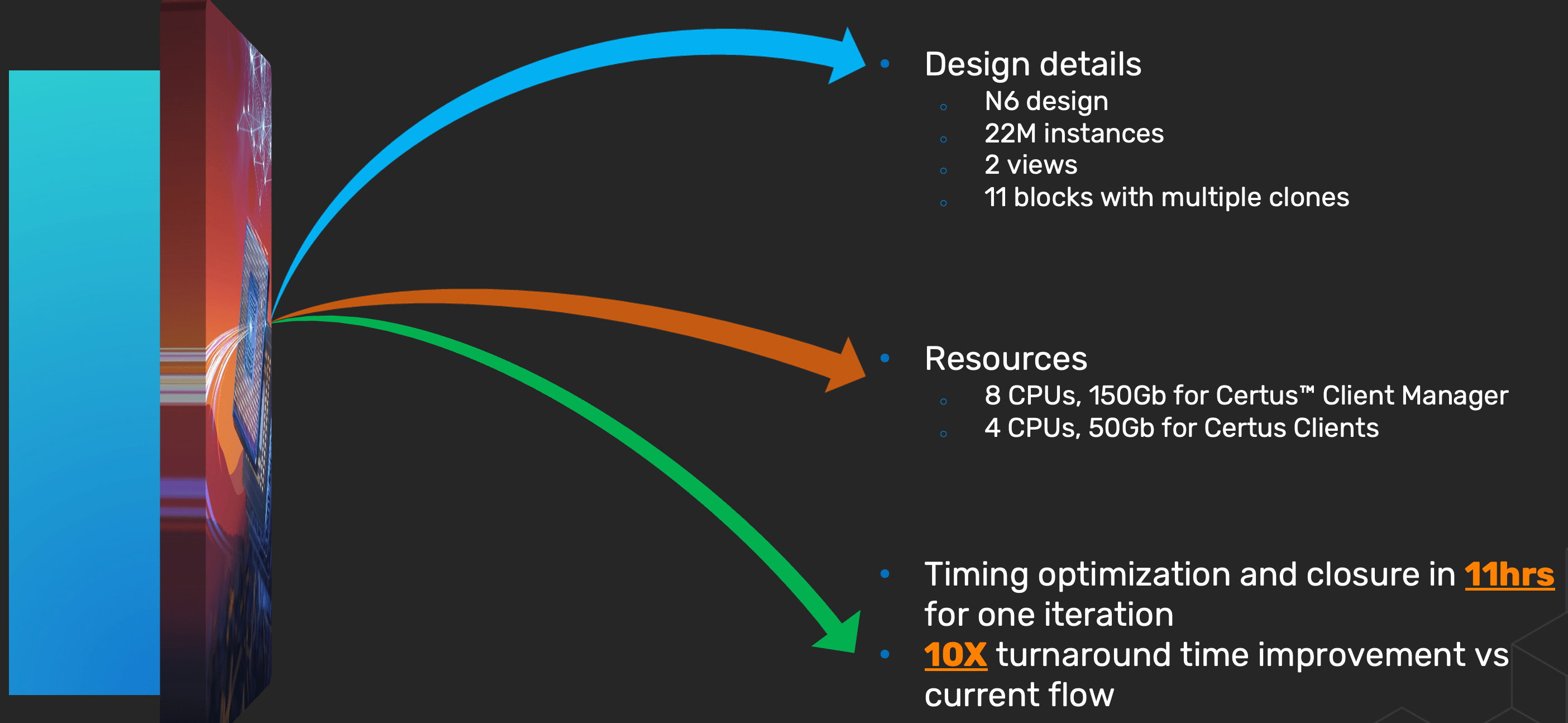 Credit: Cadence 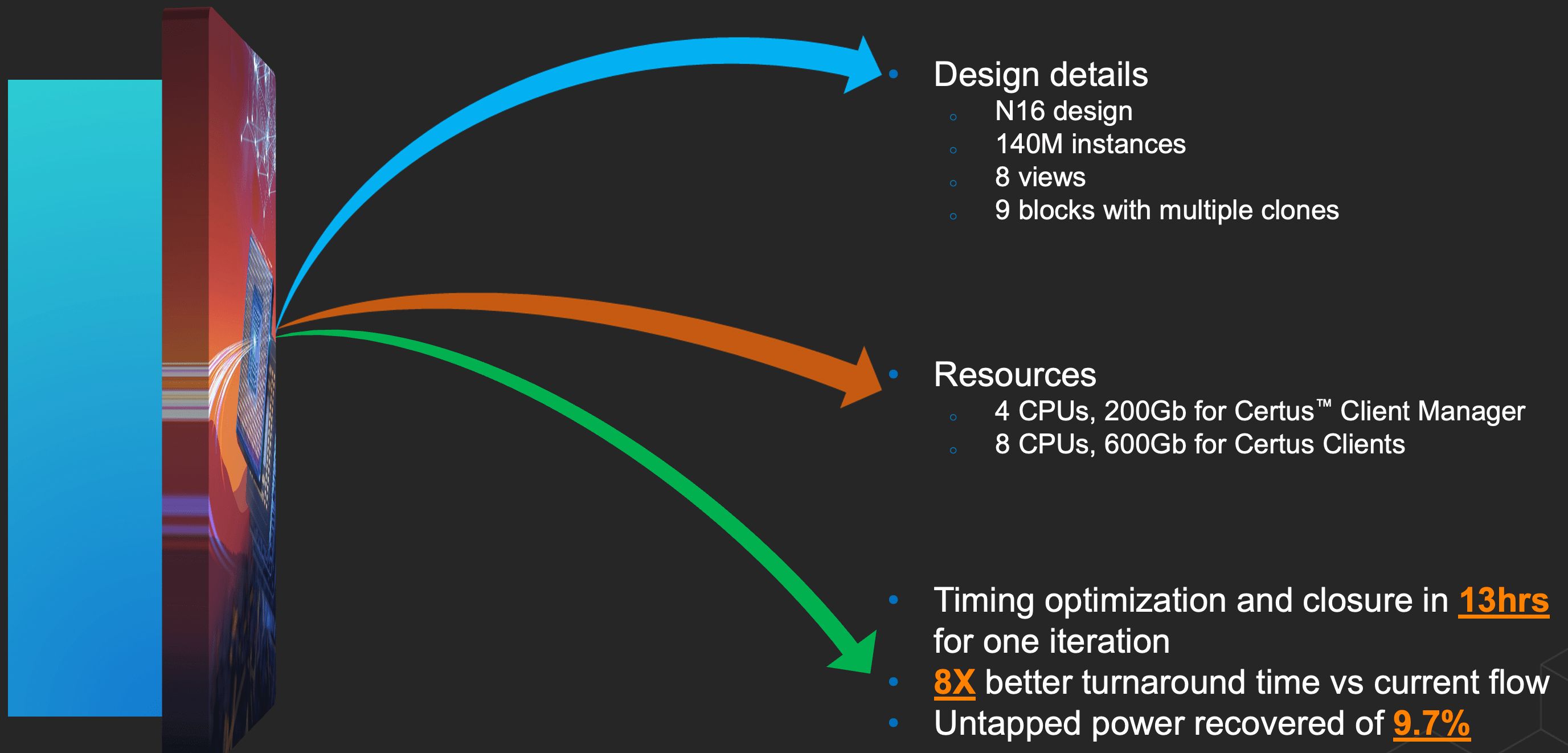 Credit: Cadence Chip-level power optimizationImproved productivity enables designers to devote time to some chip-level optimization issues that often go overlooked because of schedule pressure. “Now [with Certus] we have the capacity to also do top level power recovery. And this is very exciting because this stage in the flow typically is – I’d say historically – not often done, either for schedule pressure or due to tool issues. Now, being able to recover power at the top level really unlocks untapped power at the interfaces that previously was just left on the table. Customers are seeing several percent power recovery in their design, thanks to having this high capacity closure solution.” As Bautz explained, power recovery with Certus includes circuit-level changes, namely cell sizing and Vt swapping. Cadence maintains that Certus delivers 10%-15% inter-partition and up to 5% full chip power recovery. Usage of computing resourcesAccording to Cadence, Certus Closure Solution’s distributed hierarchical optimization and signoff architecture is a good fit for cloud-execution and is operational in both cloud and internal data center environments. Every Cadence Certus timing job is naturally multi-threaded for faster execution on minimum CPUs and memory configurations. Furthermore, Cadence claims that Certus has the unique capability to distribute optimization jobs across multiple separate machines that each take advantage of multi-threading in their own minimum memory space. Early customers reactionsThe Certus announcement quotes endorsements from MaxLinear and Renesas. Benefits cited by MaxLinear include overnight full chip-level signoff closure and power savings of up to 5%. Renesas observed 6X faster chip-level signoff closure turnaround time versus current methodologies. As Bautz pointed out, Cadence developed Certus through a collaboration with customers that “began actually multiple years ago. The product – he continued – is now fully released, and we’re positioned for multiple customer production deployment. So we’re very excited about this launch and very excited to put this product in the hands of many customers.” He added that Certus works with the latest released versions of Tempus and Innovus, both 22.1. “Certus is applicable for designs larger than a single Innovus P&R block – greater than ten million cells. This makes Certus highly applicable to ‘sub-system’ style designs (CPU, GPU, etc.) as well as full chips,” Bautz concluded. Categories: EDACafe Editorial, Video Interview |
|
|
|||||
|
|
|||||
|
|||||


 Animation, 3D Art and 3D Models")