


EDACafe Editorial Roberto Frazzoli
Roberto Frazzoli is a contributing editor to EDACafe. His interests as a technology journalist focus on the semiconductor ecosystem in all its aspects. Roberto started covering electronics in 1987. His weekly contribution to EDACafe started in early 2019. Keysight interview: signal integrity and power integrity challenges in high-speed PCB designApril 17th, 2020 by Roberto Frazzoli
EDACafe Special Report: Signal Integrity and Power Integrity Challenges in High-Speed PCB Design Part Two – Interview with Stephen Slater, Product Planning and Marketing Manager at Keysight Technologies Signal integrity and power integrity issues are becoming increasingly challenging for designers of high-speed PCBs required by next generation applications – such as 5G – and new semiconductor devices – such as DDR5 memories. What are the key aspects that designers should consider? What are the capabilities of the tools offered by EDA vendors to address these issues? To answer these questions, EDACafe has interviewed experts from some of the major vendors in this specific market. Part two of our special report features an interview with Stephen Slater, product planning and marketing manager at Keysight Technologies. On occasion of the last DesignCon show, Keysight introduced what it claims to be “the world’s first design and test workflow solution that reduces product development time for Double-Data Rate Dynamic Random-Access Memory (DDR5 DRAM) systems.” This interview will therefore focus mainly on DDR5 and on Keysight’s PathWave solution. 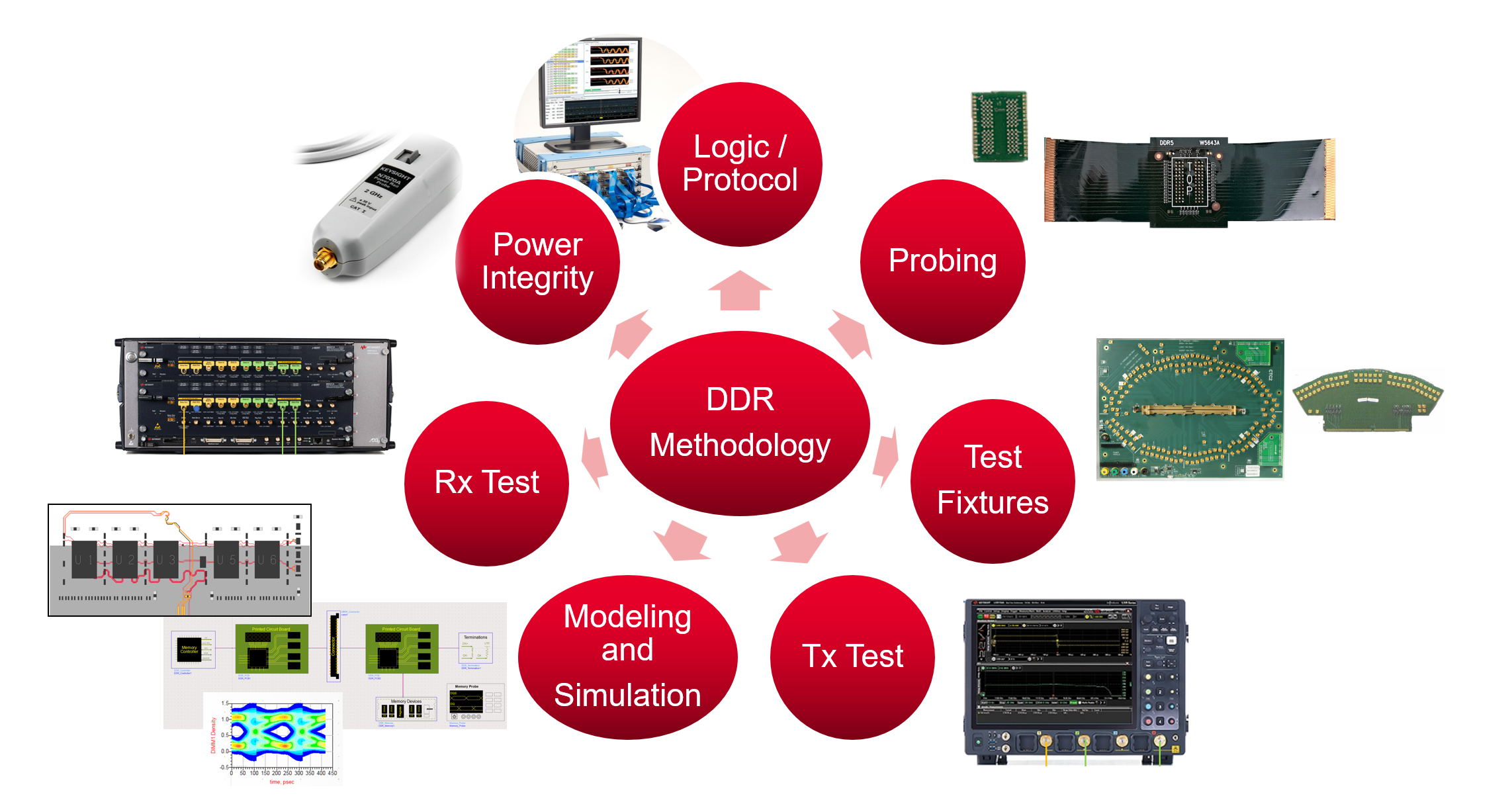 Keysight’s DDR5 complete design and test solution. Reproduced with permission, courtesy of Keysight Technologies, Inc.
EDACafe: In your view, what are the major signal integrity and power integrity challenges posed – in high-speed PCB design – by next generation applications such as 5G and by new semiconductor devices such as DDR5 memories? Can you provide practical examples of critical issues in next-generation PCB layout? Stephen Slater: DDR5 is a critical technology leap, with first generation DDR5 memories targeting a data rate of 4800 Mbps per pin. At these speeds, the PCB layout exhibits significantly more crosstalk, within a byte of data signals. The PCB designers need to not only keep the data lines length-matched (electrical length) within ps of each other, so as not to introduce skews between the signals, but they must also ensure that data bus is ‘swizzled’ – meaning data signals that are neighbors on one device, should not travel as neighbors, and end up as neighbors at the receiver. This requires more careful attention to how signals are routed, and careful attention to signal return current paths. In addition, this is the first DDR technology that expects the eye to be nearly closed at the input to the package of the receiver. Equalization (EQ) inside the receiver is intended to open up the eye, and reduce inter-symbol-interference. EQ such as variable gain amplification (VGA) and Decision Feedback Equalization (DFE) is something that is new for DDR5. Certainly, this is an exciting new development, pushing the envelope. 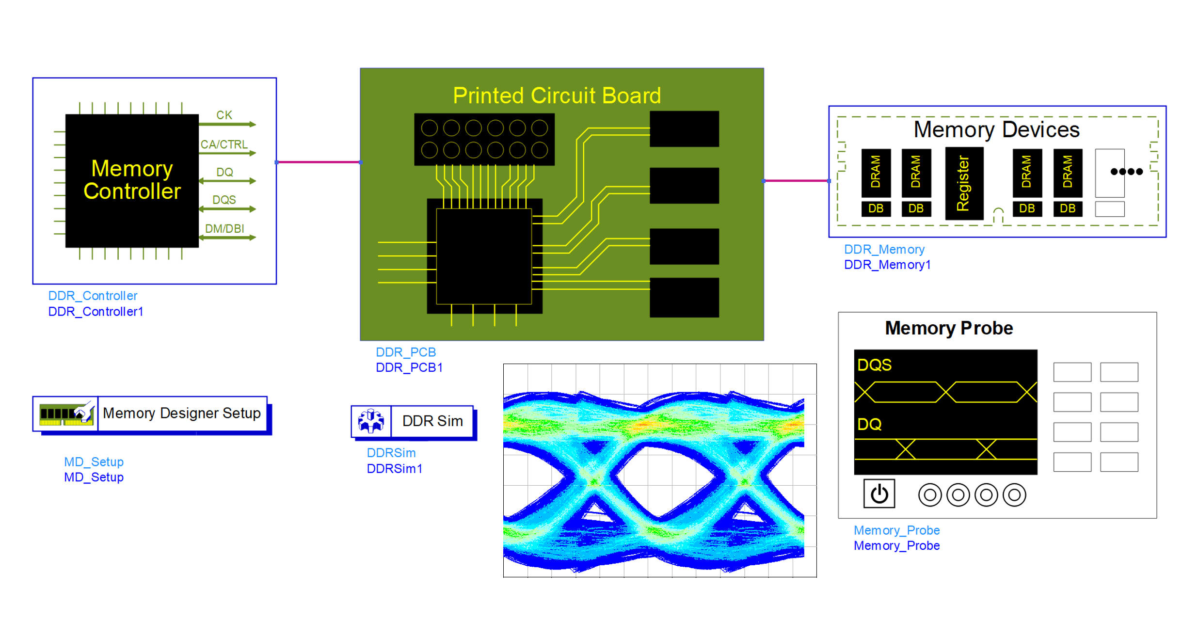 W2225BP PathWave ADS Memory Designer uses enhanced Bit-by-Bit channel simulation EDACafe: If not properly addressed, what impact could these challenges have on system performance, cost, and time to market? Is “overdesign” a common problem today? Stephen Slater: Design ‘exploration’ before jumping to layout is ever more critical for DDR5. Firstly, the SI engineer needs to work out the appropriate channel characteristics (max length, width, and spacing for traces, how many vias, the type of vias and which layers we will use to assure short via stubs), together with on-die terminations choices, and now mixing this with many new equalization controls. It means the complexity of the system becomes much greater, and to optimize the design, the need for simulation of the design upfront, becomes a necessity. Furthermore, as the unit interval of the eye is becoming smaller with each step-up in speed grade, the proportion of the eye that is eaten up by random jitter is also growing. Also, the perpetual problem of disappearing design margins. How will the system designer ensure their system offers both high performance and high reliability? The designer needs to predict, and then measure their design margin against the target system Bit-Error-Rate of 1e-16. 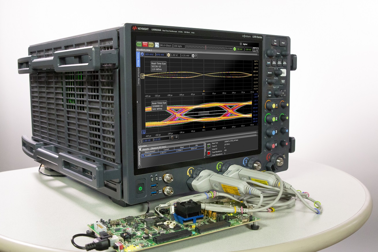 Ultra-low noise UXR series real-time oscilloscope for transmitter test, debug and receiver stressed-eye calibration. Reproduced with permission, courtesy of Keysight Technologies, Inc. EDACafe: The EDA industry is developing new approaches to tackle the new signal integrity and power integrity challenges, such as SI/PI co-simulation and the adoption of IBIS-AMI models for DDR5 memories. In your view, what are the most promising approaches? How mature are they? Stephen Slater: SI/PI co-simulation is typically enabled by power-aware IBIS models, and the electromagnetic extraction (EM) of both data line and power/ground planes. In simulation tools like PathWave ADS SIPro, these can be extracted in one single simulation, resulting in an S-parameter model that captures both signal ports and power ports in one. For DDR3 and DDR4 technologies, these types of power-aware simulations have been used frequently by designers operating close to the design limits. When it comes to DDR5 though, there are new more pressing challenges to contend with. The introduction of EQ on both transmitter and receiver means that for the first-time, silicon vendors will need to provide some capability to simulate the EQ on the device to their customers, while keeping their intellectual property secure. IBIS-AMI is the leading technology for this, which is very mature for SerDes designs, able to simulate millions of bits in minutes. DDR however, is different to high speed serial, in several respects. 1. The single-ended signals have a DC offset that we very much care about. 2. The rise-time and fall-time of a bit are different rates. 3. There is no embedded clock in DDR, there is an explicit external clock. The exact timing of the clock and the signal processing of it, will directly impact the timing of the equalization, the jitter relationships, and inevitably the eye metrics. Luckily, the three problems have already been solved, available in Keysight’s PathWave ADS Update 2. While SI/PI co-simulation has been important in the past, the focus of DDR5 right now returns to ensuring the eye has enough margin with an ideal power supply first. Power noise effects haven’t gone away, but they can be simulated and characterized as an impairment, added into the enhanced IBIS-AMI simulation flow as an additional jitter / amplitude noise. Reducing the impact, can be tackled with more rigorous Power Integrity design. 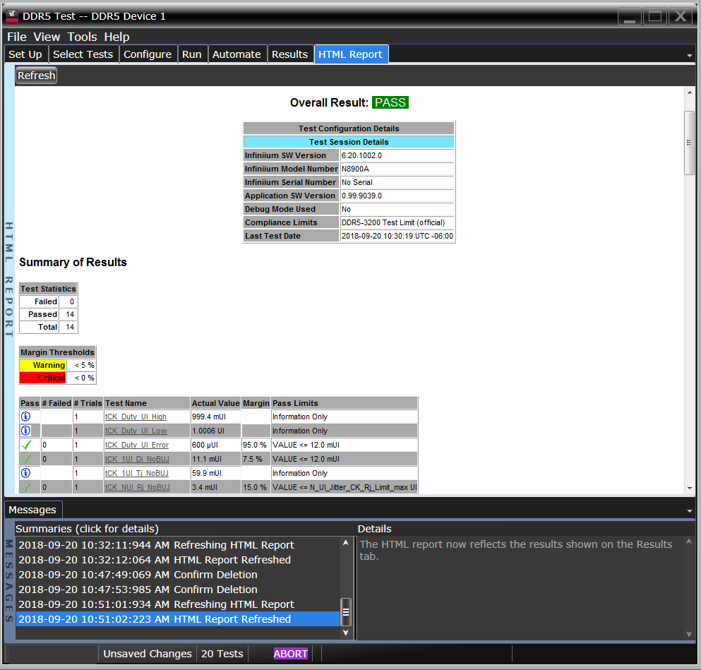 N6475A DDR5 Tx compliance test report. Reproduced with permission, courtesy of Keysight Technologies, Inc. EDACafe: Several major EDA vendors, such as your company, are already offering solutions addressing the new signal integrity and power integrity challenges. How can users choose the best solution? What features should they be looking for, when choosing a new EDA platform for this kind of application? Stephen Slater: Every designer wants three things from their design tool: the ability to predict performance of their design, in a workflow that offer greatest productivity, and delivers clear design insights (to reach an optimal design). I would ask users to look at the Keysight’s technology leadership in PathWave ADS Memory Designer, heavily featured at DesignCon 2020 – and then expand their view to encompass Keysight’s total Design and Test workflow for DDR5. This new technology wave of DDR5 has new challenges for both simulation and measurement of the final systems, and Keysight has the solutions and expertise in each of the simulation and measurement touchpoints. Keysight is poised and willing to help design teams get their products to market fastest.  N6475A DDR5 Tx compliance test report. Reproduced with permission, courtesy of Keysight Technologies, Inc. EDACafe: Briefly describe your company’s offering in this space, including the suggested design flow. Please highlight the features and benefits that set your solution apart from the others. Stephen Slater: A complete design and test workflow for DDR5 comprising: 1. Pre-layout design exploration using PathWave ADS Memory Designer, utilizing transmission line models and accurate EM extracted via models (from Via Designer). Not all tools have accurate via modeling, including the case of multiple-feed designs (as needed for command address vias). 2. Post-layout verification using PathWave ADS SIPro and Memory Designer: 2.1. optimize power distribution network designs with PIPro. Complete PI system can be solved, including behavioral modeling of voltage regulators and dynamically switching current at the point of load. 2.2. Extract signals and power/ground planes in one EM extraction with SIPro (and special DDR setup wizard). The EM technology captures signal return current paths correctly; it also captures coupling between signal vias and higher crosstalk when ground stitching vias are shared. Other hybrid techniques would miss these effects. 2.3. Run IBIS/IBIS-AMI models of the total system, in bit-by-bit enhanced channel simulation mode, using external clock waveforms to clock the DFE correctly. Other tools do not support the input of a second clock waveform into the AMI Rx model. They will not account for the jitter, or fine timing adjustment that is needed in DDR5. 2.4. Perform DDR5 virtual compliance testing with automated control over Keysight’s DDR5 Compliance App (same test software as used in real HW test). Other tools use homegrown measurement methods. 3. IBIS-AMI model generation with PathWave System Design or through model-creation consulting services. 4. Hardware transmitter tests: ultra-low noise UXR Scope, risers and interposers and probing solutions for DDR5; DDR5 compliance application; eye calibration for Rx test. 5. Hardware receiver test: DDR5 test fixture; Bit Error Rate tester for DDR5. 6. HW logic analysis / protocol debug: logic analyzer and analysis software for DDR5; protocol solution (partner: FuturePlus). 7. HW power integrity measurements: power rail current sensing probes. This concludes Part Two of our special report – the interview with Stephen Slater, product planning and marketing manager at Keysight Technologies. Next week, Part Three will feature the point of view of another major vendor of EDA solutions on signal integrity and power integrity challenges in high-speed PCB design. Related article: Interview with Wade Smith, application engineer manager at Ansys (Part One of this special report) |
|
|
|||||
|
|
|||||
|
|||||


 Animation, 3D Art and 3D Models")