EDACafe Editorial Roberto Frazzoli
Roberto Frazzoli is a contributing editor to EDACafe. His interests as a technology journalist focus on the semiconductor ecosystem in all its aspects. Roberto started covering electronics in 1987. His weekly contribution to EDACafe started in early 2019. Ansys interview: signal integrity and power integrity challenges in high-speed PCB designApril 10th, 2020 by Roberto Frazzoli
EDACafe Special Report: Signal Integrity and Power Integrity Challenges in High-Speed PCB Design Part One – Interview with Wade Smith, Application Engineer Manager at Ansys Signal integrity and power integrity issues are becoming increasingly challenging for designers of high-speed PCBs required by next generation applications – such as 5G – and new semiconductor devices – such as DDR5 memories. What are the key aspects that designers should consider? What are the capabilities of the tools offered by EDA vendors to address these issues? To answer these questions, EDACafe has interviewed experts from some of the major vendors in this specific market. Part one of our special report features an interview with Wade Smith, application engineer manager at Ansys. EDACafe: In your view, what are the major signal integrity and power integrity challenges posed – in high-speed PCB design – by next generation applications such as 5G and by new semiconductor devices such as DDR5 memories? Can you provide practical examples of critical issues in next-generation PCB layout?
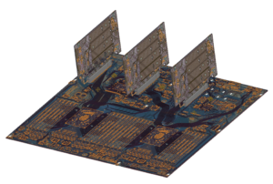
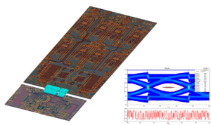
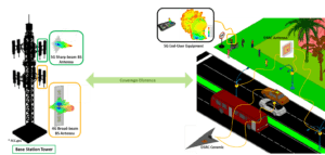
Wade Smith: There are quite a few signal integrity problems that dampen high-speed PCB designs for applications such as 5G. Material and fabrication fluctuations, increased sensitivity to noise on power planes, cables and connectors, EMI, and multi-physics are but a few issues that contribute to a degradation in high-speed signals. For example, 5G is, without a doubt, pushing datacenters to ramp up their signal processing capabilities to the levels that will support applications such as smart cities, IIoT, autonomous vehicles, next-gen healthcare, next-gen military, AR/VR applications, and more. We hear all about the need for 32 Gbps, 56 Gbps, or 112 Gbps signals being pushed around in new server applications. Signals at these speeds can be extremely sensitive to changes in materials, such as dielectric property deltas and conductor surface roughness. Fabrication tolerances that give rise to changing signal line metal dimensions or differences in electrical dielectric properties can cause the impedance a signal sees to differ sometimes up to 10% (or more depending on the material quality). Multi-physics issues, such as thermal, once thought to be a higher order problem, is now showing to cause a larger degradation on high speed signals due to its ability to alter the electrical properties of PCB materials (such as raising the metal resistivity or slightly modifying the loss tangent of dielectrics). Power plane noise from switching regulators or SSN issues can lead to issues on very sensitive low core voltages used by modern chips that handle these huge amounts of data. Also, since higher speed signals have such shorter bit times, effects such as mismatches when a signal flows through a connector are becoming an even larger hurdle. Chip packaging is another issue that is starting to plague signal integrity. New package systems are incorporating very complex interposers which need to reliably handle high-speed signals without offering too much degradation. Companies exploring the use of chiplets, HBM applications and more tend to want to cram more chips onto these complex interposers thereby leading to many signal lines that may not have a very clean reference. The combinations of these effects, in addition to other issues, are making it more and more difficult to maintain clean signal integrity. EDACafe: If not properly addressed, what impact could these challenges have on system performance, cost and time to market? Is “overdesign” a common problem today? Wade Smith: Not paying attention to fabrication tolerances and operation conditions, such as temperature, for example, can be detrimental to designs employing high-speed signals such as 16Gbps, 28Gbps, 32Gbps, 56Gbps, etc. These signals have ps bit periods, so they are easily affected by impedance discontinuities caused by changes in how the signal flows. Issues such as those discussed above can be handled by advanced simulation tools, so users can quantify the effects of these discontinuities to figure out how much their signals will be affected by them. Not doing so opens the door for design failures and re-spins that can cause hundreds of thousands to millions of dollars in fabrication costs, engineering time for lab testing/debug/redesign, increased time to market, and more. Also, depending on the application, for example health care or autonomous vehicles, poor designs that ship with potential signal/power/thermal integrity or EMI issues can lead to somebody getting seriously hurt. Overdesign typically comes into play with people are using back-of-the-napkin estimations to try to make designs work or there is a bit of inexperience in designing for projects pushing high data rate applications. However, on the other hand, I have seen some applications where underdesign was a problem due to pressure by management to cut costs, forcing engineers to use subpar materials, or a tight timeline caused engineers to rush the design. In these cases, simulation can be used in incremental stages of the design, or automation can be crafted so the simulations are automatically setup and ran thereby allowing the engineer to tackle multiple tasks in shorter time periods. EDACafe: The EDA industry as a whole is developing new approaches to tackle the new signal integrity and power integrity challenges, such as SI/PI co-simulation and the adoption of IBIS-AMI models for DDR5 memories. In your view, what are the most promising approaches? How mature are they? Wade Smith: When discussing DDR5, it is interesting to ponder the obstacles that designers will face in order to make this work correctly. First of all, DDR5 will have a faster data rate in comparison to previous DDR applications. JEDEC specs show DDR5 being capable of handling speeds up to 6400 MT/s per signal lane at 1.1V. The clock for this speed will be 3.2GHz. This means signal channel design on the PCB needs to be more sensitive and accurate than needed by slower designs in the past and bandwidths of close to 20GHz will be needed. This will push many board analysis applications into the realm of full-wave electromagnetic simulation tools. Also, it may be a good idea to model more of the channel than in past designs, so the DIMM and the DIMM connector should be included with the PCB to get a more accurate view of how the channel will affect the signal. The inclusion of multiple boards and connector models in a single simulation should help better characterize issues such as impedance mismatch, signal reflections, crosstalk, ISI, channel dispersion, and power/ground bounce are a few of the more common issues designers should expect. DDR5 applications are planned to include Decision Feedback Equalization (DFE) to help mitigate some of these effects and open the eye at the receiver chip. In this case, an SI engineer needs to have some idea of what Bit Error Rate is needed to guarantee a solid signal at the receiver in addition to voltage and timing margins. DDR5 will need a BER of 10-16. Simulating enough bits to get to a 10-16 resolution using standard transient engines with SPICE or IBIS models can take a ridiculous amount of time; hence the interest in using IBIS-AMI models. The methodology used by IBIS-AMI can greatly speed up simulation times because millions of bits are not required. These models also provide a more accurate algorithm from the vendor that characterizes their equalization methodologies. The use of IBIS-AMI models to characterize the operation of DDR5 in simulations is a great addition, however there are some issues it brings with it. One being the inability to characterize how power fluctuations will affect bit reliability. SPICE models, and more recent IBIS models, allow for the power rails to be included in the device simulation, so reference plane bounce can be added to the simulation. IBIS-AMI models do not handle this information, and DDR5 devices have a very small allowance for power plane fluctuations, so this could lead to some potential miscalculations. There are other signal characteristics required by DDR that are not currently handled by IBIS-AMI models, such as DC offset and rise/fall time differences, that may lie on the EDA simulation software to figure out how to handle. However, IBIS-AMI models being used in DDR5 applications seem to be a step in the right direction. Another area, many times not discussed, I see as a growing concern for engineers is EMI. Many engineers are trying to simulate EMI to get a better idea of how their systems will operate within more sensitive margins. One of the major areas of interest tends to be around switching voltage regulators because their switching speeds are becoming faster, thereby leading to more harmonic content in the 100’s of MHz. This not only leads to more noise in the supply rails, but also more potential for radiated emissions. This is another application for more tools that can help point out issues before engineers find them by accident in the lab. Tools such as EMI Scanners for boards can be employed at the initial phases of layout analysis to help find SI/PI/EMI issues before one advances into heavier electromagnetic simulations. Also, if needed, the power of High-Performance Computing allows for huge simulations to be completed, so users can actually place full boards in virtual anechoic chambers to run virtual EMI tests.  The ability to build full complex systems in HFSS 3D Layout that include both ECAD and MCAD structures. In this picture, a motherboard connected to multiple daughter cards via DIMM connectors. Image credit: Ansys EDACafe: Several major EDA vendors, such as your company, are already offering solutions addressing the new signal integrity and power integrity challenges. How can users choose the best solution? What features should they be looking for, when choosing a new EDA platform for this kind of application? Wade Smith: The whole idea of signal/power/thermal integrity analysis is to create a virtual prototype of a physical geometry one can use to modify and optimize in order to gain design insight while reducing the probabilities of redesigns. Weather the problem is the analysis of a 3D integrated circuit chip and packaging application, the quantization of power planes on a PCB to verify the planar impedance is at a level where it will not cause problems while supplying power to the devices in need, or the characterization of the effect a certain connector has on a 56Gbps signal, the simulation software has to be accurate. Therefore, one wants to make sure the tool of choice is reliable and well established. Tools such as ANSYS HFSS, for example, have been solving 3D electromagnetic problems for decades. This tool has been compared to a wealth of experimental data, so there is a high confidence level associated with it. There’s no arguing that sensitive electronic devices are being placed into more complex environments, so the characterization of those environments will certainly help better predict the end goal operation of the device in question. These environments could be a high-speed signal application in an autonomous vehicle which may have changing ambient temperatures depending on its location (in Phoenix in summer or Ottawa in winter). The environment may be a mini-server for a picocell 5G edge network application that sits inside a radome mounted to the side of a building in direct sunlight in Dallas. In these cases, it is a good idea to have an accurate thermal solver, such as ANSYS Icepak, that can analyze how temperatures will affect the hardware in question and feed that information back into HFSS so those effects can be taken into account in the electrical analysis. Also, I’ve noticed the physical simulations engineers are running are getting larger and larger. I wouldn’t have thought of running a full server motherboard with a press-fit connector and an IO card, all together in one EM simulation being even possible a few years ago. These types of simulations are possible with new algorithms that mix different electromagnetic solvers and make use of large compute cluster environments. If an engineer is looking to create realistic virtual prototypes that are large and complex, High Performance Computing is a must have option. Lastly, the ability to construct solutions in both the frequency and time domains is a must. In signal integrity applications, the end results usually are viewed in the time domain because the end goal is to make sure bits will travel from point A to point B. Therefore, the ability to combine the physical electromagnetic solutions with the proper stimulus such as SPICE, IBIS, or IBIS-AMI models is something that should be highly considered.  Simulation of a PCIe4 signal flowing from the CPU in a server motherboard through a press-fit connector into an IO card. Image credit: Ansys EDACafe: Can you briefly describe your company’s offering in this space, including the suggested design flow? Can you highlight the features and benefits that set your solution apart from the others? Wade Smith: In our case, we offer a full Multi-physics Chips to Cities approach. We have applications that can analyze the dynamic EM fields at the die level all the way to a full city while, at the same time, taking into effect thermal and mechanical reliability. This is a huge advantage for applications such as autonomous vehicles, electrification, modern medical designs, aerospace and defense, IoT, and 5G. We are able to offer methods of analyzing chip package system that can include a full EM simulation of a die, a package, and a board together to give the best characterization of how the channel really affects a signal. This can be extremely important for applications such as power integrity, because now you can characterize what magnitude of SSN that die actually sees (as opposed to only what is seen only on the board). Also, for signal integrity, having a unified die, package and board models can provide a better channel model than a piecemealed model, and this can be especially important for millimeter wave RF signals used in 5G applications, where impedance discontinuities can really damage a sensitive signal. We also are able to mix CAD environments, so users can pull in connectors, for example, from an MCAD model and mount them directly on a board in an ECAD environment. This allows a user to easily modify board parameters, while remaining in an ECAD environment, around a connector landing to adjust for better signal flow. Multiple boards can be linked together through connectors, and to top it off, IBIS, IBIS-AMI, SPICE, transient sources, statistical sources, and others TX/RX components can be added directly to the chip/package/board model thereby eliminating the need to create a circuit schematic. We also mix solvers in this environment, so a user can simulate entire sections using a full wave 3D solver, or the user can choose smaller sections that are more sensitive to 3D signal flow changes, and solve those with a 3D solver while solving other parts with a 2.5D EM solver. This can dramatically speed up the simulation time with a minimal degradation in accuracy. To top it all off, we can also mix physics into the solutions too, so a user can analyze the device with thermal solvers and take into account how materials will change as devices heat up, for this will affect the signal channel during high speed operation. As we leave the board, we can get into applications where antenna systems can be designed and placed into realistic environments, such as cars or cities to figure out how they will properly communicate in large environments. This helps answer questions plaguing 5G systems such as “where do I place this picocell to get the best coverage in this urban environment?” or “how is my link budget affected when my antenna heats up” or “how do I control the beam steering of my MIMO base station array so it can target track multiple autonomous vehicles simultaneously?”. In addition to this, we offer electronics multi-physics reliability applications that can assist users in assessing mean-time-to-failure of their designs in various environments with various thermal and mechanical stress conditions. In addition, solvers can be linked to large optimization engines that can help study the effects of fabrication tolerances, materials changes, or geometry manipulations. Lastly, if applicable, the use of High-Performance Computing can be employed to allow for immense simulation time speed up. Our goal is to provide the user with the most physically complete and most accurate signal channel simulation possible, no matter if the channel is just signal lines in a die, or a full 5G channel that includes an entire city. Ansys can analyze from chips to cities.  5G environment simulations taking into account multiple antennas mounted on cars, light poles, and in hand-held devices talking to a cell tower at a variable distance. Image credit: Ansys This concludes Part One of our special report – the interview with Wade Smith, application engineer manager at Ansys. Next week, Part Two will feature the point of view of another major vendor of EDA solutions addressing signal integrity and power integrity challenges in high-speed PCB design. |
|
|
|||||
|
|
|||||
|
|||||


