


There is no need to stress the impact that the current pandemic is having on every aspect and activity of the semiconductor and ICT industry. Here we will only briefly mention a couple of pandemic-related news, then move on to some of our usual market and technology updates.
Analog Devices and Infineon withdraw their market outlooks
Analog Devices “believes it is prudent to withdraw the company’s outlook for the fiscal second quarter, ending May 2, 2020,” as quantifying and forecasting the business impact of COVID-19 has become increasingly difficult. The company will provide a further update during its second quarter earnings release and call in May 2020. Infineon, for its part, is withdrawing its outlook for the whole 2020 fiscal year, citing “low visibility”. Given the uncertainty regarding the severity and the length of the pandemic`s economic impact, the German chipmaker believes that “the specific implications on sales and earnings for the 2020 fiscal year cannot be reliably assessed or quantified.”
EDA industry 2019 results
According to a report recently released by the ESD Alliance, in 2019 the EDA industry revenue reached $10.2 billion – an 8.3 percent increase over 2018. In terms of four-quarters moving average, the fastest growing EDA category was PCB & MCM with 15.1 percent, while the only slowing category was “services” with a 10.9 percent decrease. On a regional basis – again in terms of four-quarters moving average – the year 2019 saw a significant increase in EMEA and APAC (8.6 and 13.6 percent respectively), while Japan reported a 6.7 percent decrease. The Americas, EDA’s largest region, remained almost stable in 2019, with a 2.4 percent increase. Companies that were tracked by the ESD Alliance employed 45,416 professionals in Q4 2019, an increase of 6.1 percent compared to the 42,790 employed in Q4 2018.
![]()
Samsung successfully using EUV lithography for DRAM manufacturing
Samsung has announced that it has successfully shipped one million of the industry’s first 10nm-class (D1x) DDR4 DRAM modules based on extreme ultraviolet (EUV) technology. The company claims to be the first to adopt EUV in DRAM production, to overcome challenges in scaling. EUV will be fully deployed in Samsung’s future generations of DRAM, such as D1a-based DDR5 and LPDDR5 which the company expects to begin producing in volume next year. To better address the growing demand for next-generation premium DRAM, Samsung will start the operation of a second semiconductor fabrication line in Pyeongtaek, South Korea, within the second half of this year.

Samsung Electronics Hwaseong Campus (Photo: Business Wire)
Hints about El Capitan supercomputer
Last March 5th Lawrence Livermore National Laboratory, Hewlett Packard Enterprise and Advanced Micro Devices announced the selection of AMD as the node supplier for El Capitan, one of the three exascale supercomputers that the US Department of Energy plans to deploy during the next few years. The announcement provided some details, stating that El Capitan will be powered by next-generation AMD Epyc processors code-named “Genoa”, and by next-generation AMD Radeon Instinct GPUs based on a new compute-optimized architecture for HPC and AI workloads. Also on March 5th, AMD’s Financial Analyst Day offered a preview of the company’s GPU roadmap, preannouncing a “compute-optimized GPU architecture” called CDNA which will evolve into second generation CDNA 2. Now microprocessor expert Linley Gwennap has pieced together the available information to infer something more about the DOE exascale supercomputer: “[AMD] confirmed that El Capitan will feature a fourth generation Epyc processor, code-named Genoa, implemented in 5nm technology. The system will likely include the second-generation CDNA GPU. Both Genoa and CDNA 2 implement a third-generation Infinity Fabric that coherently couples the CPU with up to four GPUs. We expect CDNA 2 will use AMD’s future X3D packaging technology to combine multiple chiplets with four HBM stacks on a single substrate.” Gwennap also comments on the choice of using a single vendor for both CPU and GPU, that also applies to another DOE supercomputer which will combine Intel Xeon processors and Intel’s future Xe GPU. “This move to single-vendor CPU+GPU combinations leaves Nvidia, which dominates the world’s top supercomputers, completely out of the picture for these big American systems.”, Gwennap observes.
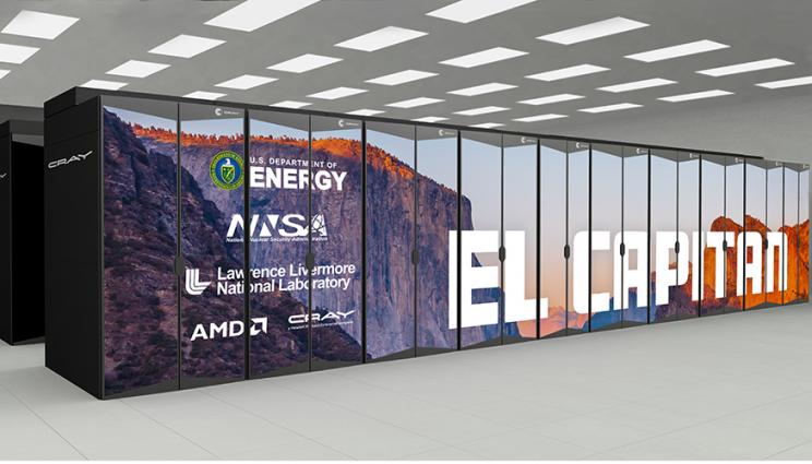
El Capitan. Image credit: LLNL
Extremely fast charging EV batteries
A new Li-ion battery technology promises to enable electric vehicles to run 400 kilometers (almost 250 miles) on a five-minute charge. Developing such a technology is Enevate, a company based in Irvine, CA, reportedly using an innovative anode consisting of a porous film made mainly of pure silicon. According to the company, the new inexpensive anode material will lead to a 30 percent increase in the range of electric vehicles on a single charge. Enevate’s patented process creates the porous 10- to 60-µm-thick silicon film directly on a copper foil, and includes a nanometers-thick protective coating to prevent the silicon from reacting with the electrolyte. Enevate claims that its roll-to-roll processing techniques reduce cost compared to graphite anodes and allow high-volume manufacturing. Energy density can also be increased: the company has made battery cells reaching 350 watt-hours per kilogram. Enevate is reportedly working with multiple major automotive companies to develop standard-size battery cells for electric vehicles hitting the market in 2024-2025.

Benjamin Park, Enevate’s founder and CTO. Image credit: Enevate
Small global-shutter image sensors from STMicroelectronics
Global-shutter image sensors save all pixel data in each frame simultaneously, as opposed to “rolling-shutter” operation that captures pixel data sequentially one line at a time – not the best option with moving images. Now two new global-shutter image sensors from STMicroelectronics claim high speed and very small die size. The new sensors are the VD55G0 with 640 x 600 pixels and the VD56G3 with 1.5 Mpixels (1124 x1364), measuring 2.6mm x 2.5mm and 3.6mm x 4.3mm respectively. ST claims low pixel-to-pixel crosstalk at all wavelengths, ensures high contrast for superior image clarity. Embedded optical-flow processing in the VD56G3 calculates movement vectors, without the need for host computer processing. Key to these performances is ST’s advanced pixel technology, including full Deep Trench Isolation (DTI), that enables extremely small 2.61μm x 2.61μm pixels. The ST approach allows space-saving vertical stacking of the optical sensor and associated signal-processing circuitry on the bottom die. Integrated digital circuitry incorporates hardware features including an exposure algorithm, automatic defect correction, and automatic dark calibration. These new sensors are suited to applications such as Augmented and Virtual Reality (AR/VR), Simultaneous Localization and Mapping (SLAM), and 3D scanning.


 Animation, 3D Art and 3D Models")