
Posts Tagged ‘SoC’
Monday, July 19th, 2021
In my last post, I mentioned that Agnisys is currently in the middle of a series of new webinars on how specification automation benefits many teams developing intellectual property (IP) blocks and system-on-chip (SoC) designs. When we first started supporting register and memory automation, we focused on generating register-transfer-level (RTL) design descriptions and Universal Verification Methodology (UVM) simulation testbench models from executable specifications. You generate these outputs as soon as the specifications are ready and re-generate them every time that the specifications are updated throughout the project.
This is of clear benefit to design and verification engineers. The designers never have to write any RTL code for registers or memories, or update code manually when requirements change. Similarly, the verification team developing the UVM testbench for the IP or SoC incorporates the generated models without having to develop them by hand, and automatically updates them when needed. When we added sequence automation to our product family, we helped the UVM effort even more. Over time, we’ve added design and verification generation for a wide range of standards-based IP as well as SoC-level interconnection of IP and custom blocks.
(more…)
Tags: SemiEDA, SoC, SystemRDL, UVM
No Comments »
Wednesday, June 23rd, 2021
If there’s one good thing to emerge amid all the challenges of the last year and a half, it’s improved technology for remote learning. On-line talks, webinars, and podcasts are nothing new, but with so many people working at home the importance of virtual options has grown. When was the last time you had a vendor physically visit your company in person to talk about a new tool or technology? When was the last time you attended an in-person conference or seminar? For many engineers, it has been well over a year since we were even in the office. We’ve relied on the web for just about everything.
At Agnisys, we’ve been doing regular webinars since well before the pandemic and they have been highly effective and successful. We offered a series last year that proved quite popular, and you may have noticed that we recently announced a new series that began a few weeks ago. With interest in remote learning at an all-time high, we fully expect a great turnout for all our upcoming virtual events. Even if you’ve attended some of our webinars before, I encourage you to check out our new series because we’re taking a dramatically different approach to the material.
(more…)
Tags: RTL, SoC, SystemRDL
No Comments »
Monday, September 28th, 2020
A couple of years ago at the Design Automation Conference (DAC), as I walked the exhibit floor I was amused by how many EDA vendors had jumped on the marketing bandwagon for artificial intelligence (AI) and machine learning (ML). Many company slogans, booth posters, and demonstrations claimed that AI/ML techniques had been incorporated into their products. Doubtless some of these claims were true, but for certain companies and product categories it was hard to believe. In this post, I’ll discuss a real use of AI/ML technology at Agnisys, already implemented and available to users now.
Let’s start by defining a few terms. AI is a broad description referring to any computer program that automatically does something that would traditionally have required human intelligence. AI works at its best by combining large amounts of data with fast, iterative processing and intelligent algorithms. ML is a subset of AI using advanced techniques and models that enable computers to figure out interesting things from the datasets and deliver AI applications. Along with the algorithms, what is most important for AI/ML is the quality and quantity of the data used to train the model for these algorithms.
(more…)
Tags: SoC, testbenches
No Comments »
Tuesday, August 4th, 2020
In my last blog post, I talked a bit about the history of the annual Design Automation Conference (DAC) and mentioned that this year it would be a virtual event due to the ongoing pandemic. The show concluded about ten days ago and so we’ve now had time to assess the results. I thought that some of you who were unable to attend might be curious how it went, so I’d like to provide a quick summary.
The first thing to say is that virtual events are still novel and a bit daunting for both exhibitors and attendees. This was the first virtual show for Agnisys, so it took some adjustment to our usual preparation and promotional efforts. The good news is that we had an impressive number of visitors to our DAC virtual booth, so lots of you were able to find out about us, our products, and our customers. We also had a quiz that proved quite popular. The less-good news is that some visitors didn’t navigate to the deeper engagement options. It seemed that the concept of the virtual booth was unclear, plus many users (including our own engineers) were stymied by technical issues on the DAC site.
(more…)
Tags: Allegro MicroSystems, Analog Inference, ARV, dac, IDS, ISS, SLIP-G, SoC, SoC-E, Yellowbrick
No Comments »
Monday, June 29th, 2020
System-on-chip (SoC) projects are, by their very nature, complex and difficult to complete successfully. Specification, architecture, design, and verification are all challenging. This blog post focuses on the challenges faced by designers, driven by the convergence of applications onto a single SoC device. This increases the demand for design functionality and design performance. At the same time, market requirements generate pressure to drive down the cost of design and meet shrinking market windows due to shorter product shelf lives. Every step of the design process has become more difficult, even the seemingly simple task of assembling all the pieces that make up the SoC.
Today’s large chips may contain 500 of more instances of intellectual property (IP), a combination of new designs, reused blocks from previous projects, and licensed commercial IP. If each of these blocks averages 50 ports, then 25,000 connections must be made among them. Making these connections manually is tedious and time-consuming, with a high chance of errors. Meeting cost and schedule goals requires a big increase in the productivity of the SoC design team. Methodology improvements are needed to help accelerate assembly of chips and systems through automation.
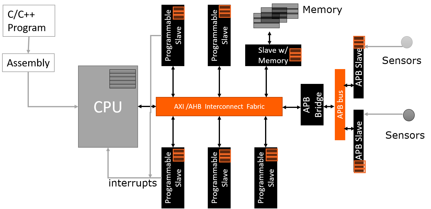
The best solution is providing designers flexible, customizable, and configurable IP and subsystem generators along with a tool to automate architectural level SoC assembly and connectivity. The capabilities for such a solution include:
- Creating and editing the design on the fly through scripts or a command line interface
- Generating major subsystems with flexibility to customize or configure
- Automatically adding instances to the design, making connections, restructuring, etc.
- Viewing the resulting schematics for design analysis
- Running design rule checks to endure IP and SoC quality
- Generating appropriate files for design, verification, and software teams
(more…)
Tags: SoC, SoCdesign, System-on-chip
No Comments »
Monday, October 7th, 2019
The idea of an open-source CPU core was virtually unheard-of ten years ago – let alone using it for commercial applications. The CPU core has been the most critical part of any computing system and thus, has been the most valuable and profitable. Over the years, companies like IBM®, Intel® and ARM® have built their empires either from CPU core development or license distribution.
Fast forward to today, the entire computing industry is in the early stages of a new paradigm shift where the CPU would no longer be the central processing unit. Mainly driven by the exploding growth of data that we produce and consume as a global society, even the highly successful von Neumann architecture is becoming obsolete. There is big data used for prediction, analytics and machine learning training, and there is fast data used for real-time applications such as IoT edge, geo-spatial systems and autonomous vehicles.
(more…)
Tags: DVCon, IDesignSpec, IoT, ISequenceSpec, machine learning, RISC-V, SoC, test sequences, UVM
No Comments »
Friday, August 16th, 2019
By Louie De Luna, Agnisys Chief Product Evangelist
The conventional von Neumann architecture has been the workhorse of computing for several decades, but with the advent of AI applications and big data the entire industry has put a spotlight on its limitations. Since massive amounts of data need to travel back and forth between the CPU and memory, the resulting latency and power consumption became major issues. One of the powerful convolutional neural networks (CNN), Alexnet, requires 68M total weights (parameters) and 724M total MACs for a single inference process – a mere average requirement compared to other CNNs such as VGGNet which requires 138M total weights and 15.5G total MACs.
New chip architectures and technologies are now emerging to address these issues known as the “von Neumann bottleneck” or the “memory wall” problem. The Google TPU is based on systolic arrays that provides up to 420 Teraflops, the Graphcore IPU is based on Bulk Synchronous Parallel (BSP) technology that provides up to 125 Teraflops and IBM Zurich Lab is working on a new AI chip based on in-memory computing.
But as the world of computing and AI wait for the new chip architectures to mature, the memory wall problem is still a real pain. Startups without the backing of deep pockets will need to come up with other ingenious ways in order to be competitive.
(more…)
Tags: AI, hotchips, IDesignSpec, SoC, Verification, vonNeumann
No Comments »
|


 Animation, 3D Art and 3D Models")