Siemens EDA Juergen Jaeger
Juergen Jaeger is the director of prototyping product strategy for Simens EDA. Prior to joining Siemens, Juergen was the director of product management at Cadence Design Systems, responsible for all FPGA-based prototyping activities. Prior to that he worked at Synopsys via the acquisition of … More » FPGA-based prototyping – to build, or to buy, that is the question!December 20th, 2024 by Juergen Jaeger
Almost as long as FPGAs have been around, they have been used to prototype ASICs, SoCs, and IPs. While initially, the only option for users was to build their own prototyping board, that quickly changed with many commercial prototyping boards becoming available from vendors large and small. Ever since, the large question for users has been, should I develop and build or buy my boards? Now, consider the pros and cons of this “build vs. buy” debate. But before that, probably the first question to ask yourself is what do you want the FPGA-based prototype to do? Having that answer allows you to consider the right priorities and trade-offs inherent in the decision to build or not to build a board. Let’s assume you buy rather than build, which commercial solution should you purchase? Key questions to ask yourself here are:
Read the rest of FPGA-based prototyping – to build, or to buy, that is the question! Siemens’ Next-Gen Electronic Systems Design Platform: A Unified Vision of AI, Collaboration, and InnovationDecember 16th, 2024 by Sanjay Gangal
In a transformative leap for electronic systems design, Siemens Digital Industries Software has unveiled a next-generation platform that integrates its industry-leading tools—Xpedition™, Hyperlynx™, and PADS™ Professional. This groundbreaking release is more than a mere product update; it represents a holistic reimagining of the design process, aimed at solving critical challenges in a rapidly evolving industry. I had the privilege of speaking with AJ Incorvaia, Senior Vice President of Electronic Board Systems at Siemens, who shared the philosophy and features driving this ambitious project. According to AJ, “This is the platform that we will be building on for years to come, combining the power of AI, seamless cloud connectivity, and a unified user experience to empower engineers and organizations.”
The electronics industry faces multiple hurdles: a wave of experienced engineers retiring, less experienced talent stepping in, growing design complexity, and supply chain instability. These factors demand tools that are intuitive yet powerful, fostering collaboration across increasingly globalized and multidisciplinary teams. To address these challenges, Siemens has unified its PCB design tools into a single cohesive platform. The new system not only integrates layout, schematic capture, and signal integrity analysis but also connects seamlessly with Siemens’ Teamcenter® for product lifecycle management and NX™ for mechanical engineering. This cross-domain collaboration ensures that electrical and mechanical engineers can work in harmony, solving a historically difficult problem of mismatched terminology and disconnected workflows. Enhance power reliability through design-stage layout optimizationNovember 22nd, 2024 by Sanjay Gangal
As integrated circuit (IC) designs continue to scale, the demand for efficient power management, optimized performance and reliable physical layout modification grows more critical. Meeting power, performance, and area (PPA) targets is essential for effective IC operation at advanced process nodes. However, design and verification engineers face challenges in addressing issues like IR drop and electromigration (EM) early in the design process without compromising PPA objectives. This is where a shift-left approach to power grid optimization can make a significant difference. By making design-stage layout modifications, designers can proactively tackle power management issues, enhancing reliability and PPA metrics. This strategy not only benefits engineering teams but also delivers substantial business advantages by reducing rework, lowering costs and accelerating time to market. Read the rest of Enhance power reliability through design-stage layout optimization Multi-FPGA Partitioning – What’s the Recipe for Success?November 12th, 2024 by Romain Petit
Multi-FPGA partitioning has undergone significant advancements over the years, driven by the increasing complexity of digital systems and the need for efficient prototyping and verification. Today’s prototypes require dozens of the larger FPGAs available in the market; making an optimized and automated approach to FPGA partitioning essential. Partitioning designs across multiple FPGAs was often done manually. Engineers would divide the design based on their experience and intuition, which was time-consuming and prone to errors. This method worked for simpler designs but became impractical as the complexity of systems grew. As digital designs became more complex, automated partitioning tools were developed. These tools aimed to optimize the partitioning process by considering logic capacity and inter-FPGA communication. Hierarchical partitioning divides the design into smaller, manageable blocks, and then partitions them further. This method improves the efficiency of the partitioning process and reduces execution time. Read the rest of Multi-FPGA Partitioning – What’s the Recipe for Success? Revolutionizing Debugging with Veloce proFPGA CS: Unleashing Full Visibility with the First FPGA VP1902 Powered Software Prototyping SystemOctober 4th, 2024 by Romain Petit
The semiconductor industry is witnessing an exciting breakthrough with the introduction of Veloce proFPGA CS, the first VP1902 FPGA-based software prototyping solution on the market. Beyond its remarkable architecture, modularity, scalability, and high performance, Veloce proFPGA CS sets itself apart by prioritizing the designers experience. In this article, we explore Veloce proFPGA CS and its full visibility debug capabilities, driven by innovative and unique reconstruction algorithms. This functionality has redefined the way designers approach debugging. Additionally, we delve into the seamless integration of backdoor access for memories allowing quick experiments with different application scenarios. In today’s era of rapidly advancing design complexity, traditional probe-based debugging methods are no longer sufficient. While probe-based debug may provide limited visibility to register signals, it lacks the granularity required for detailed analysis of all signals. This shortcoming hinders the ability to identify the root cause of bugs quickly and accurately. And as designs become more intricate with hundreds of interconnected components, the need for a comprehensive view of the systems behavior has become critical. The innovative reconstruction algorithms offered by proFPGA CS enables visibility to the cause of bugs. Unleashing Full Visibility:
Chip-level thermal analysis solves a main barrier to 3DICsSeptember 12th, 2024 by Lee Wang
As the semiconductor industry adds more functionality into smaller footprints, we are pushing the boundaries of traditional two-dimensional integrated circuit (2DIC) designs. The next phase in the growth of performance and functionality is building three-dimensional integrated circuits (3DICs). However, this new dimension introduces a host of challenges, the most significant of which is managing heat dissipation. The allure and pitfalls of 3DICs The advantages of stacked dies interconnected using vertical interconnect accesses (vias), to create a single, compact package include:
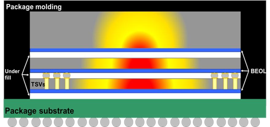
To realize these benefits, designers first need to clear some key hurdles, including the significant challenge of managing heat dissipation (figure 1). Because 3DIC architectures are so compact, heat generated by the densely packed components can cause hot spots that affect performance and reliability.  Figure 1. Illustration of a 3DIC with heat dissipation. Read the rest of Chip-level thermal analysis solves a main barrier to 3DICs Veloce proFPGA CS Changes the Game for Software PrototypingSeptember 9th, 2024 by Gabriele Pulini
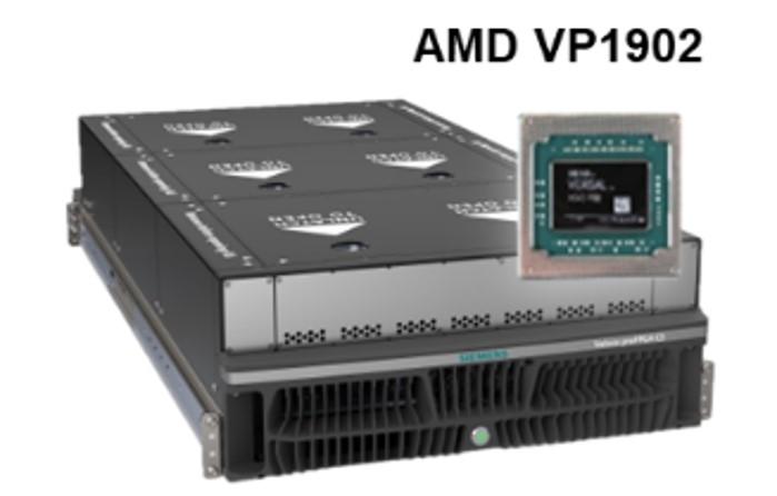
With the AMD VP1902 FPGA device boasting double the capacity, you unlock a whole new level of performance and cost-effectiveness.
Performance. You can map more of your design onto a single chip. This means that fewer FPGA devices are needed overall, resulting in streamlined mapping and improved performance. The benefits extend beyond performance. With fewer FPGA devices required, the cost per gate for your prototyping platform plummets. That’s right – 50% lower cost per gate means significant savings for your budget. You can achieve more with less, maximizing the performance of your resources. Consolidation: Mapping your design onto a single high-capacity FPGA simplifies the setup and configuration process. No more juggling multiple devices or dealing with complex interconnectivity. Simplifying setup and configuration means faster and more efficient prototype bring-up, allowing you to accelerate your development cycle like never before. You have more opportunities to test different scenarios, catch potential corner case issues, and optimize the quality of your design. To learn more, download the Veloce proFPGA CS factsheet or email Romain Petit romain.petit@siemens.com for details. FPGA-Based Prototyping – from “Do-It-Yourself” to an Essential SoC Verification and System Validation ToolAugust 26th, 2024 by Juergen Jaeger
Then chip designs exploded in complexity, software content increased exponentially, and the sheer amount of data going in and out of an SoC grew by orders of magnitude. And let’s not forget that design cycles shrank at the same time. FPGA-based prototype platforms, uniquely suited to address those challenges, have become essential to SoC verification and system validation. As all this change was happening, prototyping evolved as well. Today it is no longer a construction kit, but a ready-to-use, comprehensive solution that delivers significant productivity gains. You might ask, what are the primary attributes of this evolved FPGA-based prototyping platforms? Obviously, it’s hardware consisting of one or more FPGAs! It’s also the software that takes the ASIC RTL and intelligently maps it into the collection of FPGAs. It’s also a test environment that stimulates the design, often with live system interfaces like sensors, cameras, and ethernet traffic. Accelerating your simulation runs. Bridging the simulation and emulation gap using Veloce sim-accel methodologyAugust 12th, 2024 by Saurabh Jain
Welcome to the world of Siemens Hardware Assisted Verification (HAV) engines, a fast-paced verification ecosystem that synthesizes the design and a large part of the testbench and then maps it to the Veloce Hardware. This setup runs 1000 to 10000 times faster than a simulator. Roughly, the same design that took days and weeks now runs in minutes. That’s incredible, isn’t it?
Now, such a system is like a relay race. The slowest player can significantly impact the overall performance. The obvious solution is to assign the shortest lap to the slowest player. Simulators are painfully slow in the relay race of Emulators and Simulators. How do we further reduce the time spent on simulators? The Siemens Veloce team took a multi-pronged approach to provide a solution. First, Veloce provides a rich set of Veloce transactor libraries (VTLs) of standard protocols and soft memory models. These VTLs are emulation-ready, geared towards performance, and support plug-and-play. A user simply replaces the simulation Verification IP (VIP) with an equivalent Siemens VTL to migrate a large portion of the design. The VTLs cater to large industry segments such as networking, automotive, storage, video, mobile/smartphone, and 5G, to name a few. Supercharge Your HAV Investment with Veloce ES (Enterprise Server) AppJuly 29th, 2024 by Chenguang Li
In today’s fast-paced world of hardware design and verification, accelerating time-to-market and optimizing resources are paramount. Hardware-Assisted Verification (HAV) significantly reduces verification time, allowing hardware design teams to meet tight deadlines and bring products to market faster. Moreover, HAV enables thorough testing of intricate designs, uncovering potential issues early in the development cycle and ensuring product reliability. While HAV represents a significant investment and offers numerous benefits, managing multiple projects, diverse teams, and varying job priorities on a shared HAV platform can be overwhelming. Enter the Veloce Enterprise Server (ES) App – a revolutionary solution developed by Siemens EDA to streamline Veloce hardware resource management and transform the HAV landscape. Understanding Hardware-Assisted Verification
However, managing the efficient use of HAV resources, especially when dealing with multiple projects and teams, poses significant challenges. This is where the Veloce ES App comes into play. Read the rest of Supercharge Your HAV Investment with Veloce ES (Enterprise Server) App |
|
|
|||||
|
|
|||||
|
|||||


 Whether pushing the boundaries of SoC verification, validating complex IP blocks, or simulating massive software workloads, the Veloce proFPGA CS software prototyping platform, equipped with the VP1902 FPGA device, doubles the capacity and delivers verification success.
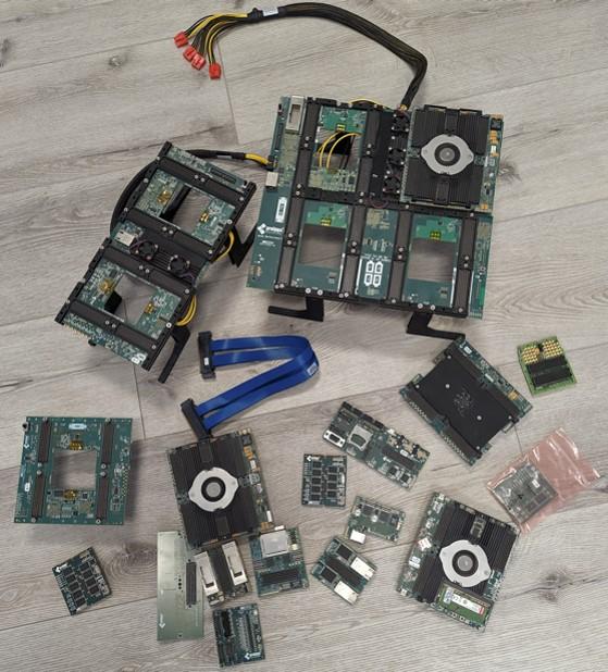
 FPGA-based prototyping has always been something of an assembly-required construction kit. Consequently, getting to a functional and usable prototype took a lot of effort, time, and a ‘do it yourself’ attitude. Once up and running, however, the reward justified the effort by providing a fast pre-silicon verification platform, with frequencies often running at tens of megahertz and reducing verification workload runs from days to minutes.
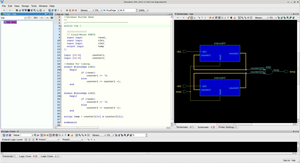
 A verification environment typically has a design under test (DUT) surrounded by verification-driven constructs. No synthesis tool can synthesize every supported keyword. Design engineers are always careful with limiting themselves to using synthesis-friendly constructs. Verification engineers are more fluid because they do not worry about synthesis. Emulators are no exception. They can synthesize the design, but the testbench runs on a host machine. The two communicate through interfaces or established standard protocols.
  Hardware-Assisted Verification (HAV) uses dedicated hardware to accelerate the verification process of semiconductor designs. This approach allows for faster execution of test cases compared to traditional software-based simulations, significantly speeding up the verification cycle. HAV is particularly beneficial for large and complex designs, where traditional simulation methods fall short in terms of speed and capacity. For more information on Siemens EDA HAV, see the article,


