In an industry accustomed to incremental change, Veloce CS is a departure because it is a complete three-in-one system, a development that Ron Wilson, a longtime technology editor, explores with Brunet in this 2 part blog.
Wilson: What is Siemens’ value proposition?
Brunet: Low cost of purchase and operation, seamless fit into the datacenter and shareability define the value proposition for the Veloce Strato CS and Veloce Primo CS systems at the enterprise level. Also, high performance and fast model compiles, scalability to 44-billion gates and congruence—commonality of RTL models, operation, and databases for the two systems extended to include the at-speed proFPGA CS system.
One command language. One design model. One database. The Veloce CS system meets the challenges of this leading-edge designs generation and the next. The technology we use to build the Veloce CS system changed since our previous generation of systems. FPGAs in Veloce Primo CS and Veloce proFPGA CS prototyping systems and the custom programmable chips in the Veloce Strato CS emulation system have higher capacity, greater speed and lower power consumption. We exploit 2.5D multi-die module technology and optical interconnect.
 Wilson: How do you differentiate between the three?
Brunet: Although the three systems are united by common user interface, RTL models and database, each must meet the demands of its role in the design process. Each has distinct attributes and is implemented in a different way.
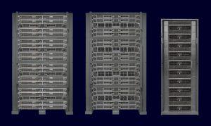
Capacity is a requirement because of enormous gate counts. Emulation and enterprise prototyping systems must be able to hold the entire compiled RTL model for the chip to observe real workload execution. Veloce Strato CS and Veloce Primo CS offer fine-grained, plug-in scalability from entry-level up to the equivalent of 45-billion gates through advanced ASIC processes and, for prototyping, advanced FPGAs, use of high-speed interconnect, and a modular architecture.
Speed is needed to exercise an entire chip design and execute real workloads. Veloce Strato CS exploits its new ASIC and interconnect. Veloce Primo CS uses advanced FPGAs and interconnect to give it execution speed greater than Veloce Strato CS.
Large models also require fast compilation. By developing our RTL model compilers in parallel with the internal architectures of Veloce Strato CS and Veloce Primo CS, we sped up compilation times and avoided problems that slow compilation. Recompilation will be fast when the RTL model needs to change.
Another need is fast, understandable trace and trigger operation, reflected differently in each. During emulation, designers are typically interacting in detail with the RTL, observing logic signals. Veloce Strato CS makes all signals in the model available to trace, trigger or breakpoint commands. FPGA-based Veloce Primo CS and Veloce proFPGA CS systems require access to individual signals to be specified when the model is compiled. Software developers, who typically interact with workload source code and variables, get the added speed of the FPGA-based architecture in exchange for less ways to change their access to logic-level signals.
The processes of compiling the RTL model for Veloce Strato CS and Veloce Primo CS are nearly identical. A switch directs the compiler to one system or the other while the model stays the same. Veloce proFPGA CS uses the same RTL model.
Congruence ensures teams can share a single RTL model to work together or separately and communicate efficiently. An RTL model will compile to produce the same behavior in each system at different execution speeds and levels of observability, even though the compiled code will be different for each. The same user command will produce the same result on Veloce Strato CS and Veloce Primo CS and on Veloce proFPGA CS when the context makes sense.
The Veloce CS system features directly relate to the needs of design teams because enterprises need the ability to share naturally and easily between members of the same project and across enterprises.
Software configurability is important, too. Different teams work on different RTL models of different sizes, a given for emulation systems. Configurability via software comes at a cost for enterprise prototyping systems. The speed of the links between FPGAs is critical to overall system performance. The fastest links are hard-wired or are pluggable cables. Both inhibit flexibility. Allowing a design team days of access to an enterprise prototyping system in a remote datacenter to reconfigure cables is difficult for logistical and security reasons.
Granularity is an issue for energy and capital efficiency.
Veloce Strato CS and Veloce Primo CS platforms drop seamlessly into enterprise datacenters and comply with footprint standards for datacenter racks using standard cabling conventions for power and networking. Veloce proFPGA CS is physically smaller than enterprise systems and is designed for benchtop use in a lab as well as rack based for datacenter with the hexa blade offering.
Wilson: How can our readers get more information?
Brunet: I invite them to download the Veloce CS System whitepaper.


 A company uses AI and ML to design its chips and they are not designed by hardware engineers. Because everything starts with a software driver, software defines the product. This new type of user is not taking the derivative of a whole design for targeted chips to address a specific market or application. In this design flow, hardware design is started only after the system specification is defined.
 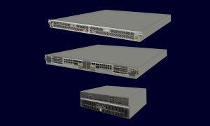 Brunet: The Veloce CS system is architected for congruency, speed and modularity and supports design sizes from 40-million gates to designs integrating more than 40+ billion gates. It executes full system workloads with elevated visibility and congruency, enabling teams to select the right tool for a task’s unique requirements for faster time to project completion and decreased cost per verification cycle.


 Animation, 3D Art and 3D Models")