Siemens EDA Sanjay Gangal
Sanjay Gangal is the President of IBSystems, the parent company of AECCafe.com, MCADCafe, EDACafe.Com, GISCafe.Com, and ShareCG.Com. Enhance power reliability through design-stage layout optimizationNovember 22nd, 2024 by Sanjay Gangal
As integrated circuit (IC) designs continue to scale, the demand for efficient power management, optimized performance and reliable physical layout modification grows more critical. Meeting power, performance, and area (PPA) targets is essential for effective IC operation at advanced process nodes. However, design and verification engineers face challenges in addressing issues like IR drop and electromigration (EM) early in the design process without compromising PPA objectives. This is where a shift-left approach to power grid optimization can make a significant difference. By making design-stage layout modifications, designers can proactively tackle power management issues, enhancing reliability and PPA metrics. This strategy not only benefits engineering teams but also delivers substantial business advantages by reducing rework, lowering costs and accelerating time to market.
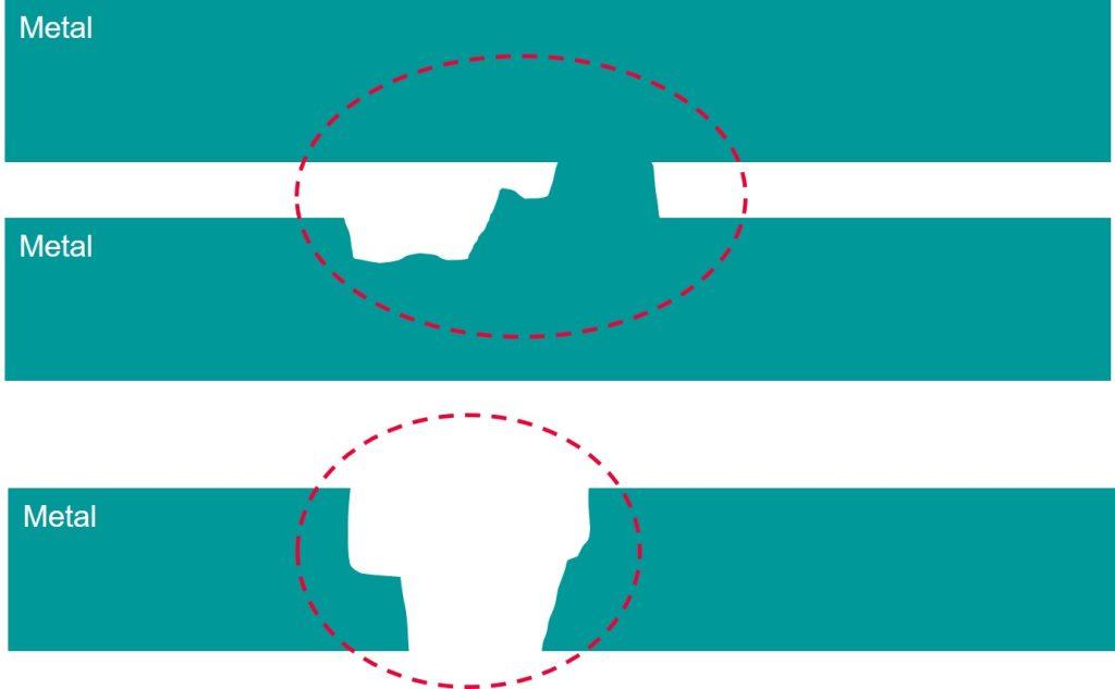
The need for design-stage layout modifications In any IC design, maintaining an optimal power distribution network is a fundamental requirement. IR drop and EM can significantly impact an IC’s reliability and performance (figure 1). Traditional approaches to address these issues tend to be reactive, with modifications and adjustments taking place during signoff verification, leading to longer design cycles, delayed schedules, and higher costs.
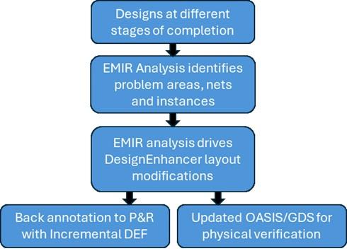
Figure 1. EM can create short circuits between two interconnects through the development of hillocks, or an open circuit through the creation of voids. Shifting power grid optimizations to the design implementation stage rather than waiting until signoff allows design teams to anticipate and mitigate issues like IR drop and EM earlier. This shift-left methodology supports correct-by-construction layout enhancements, resulting in a smoother design flow and improved EMIR outcomes. Key layout modification techniques Modern layout modification tools, like Calibre DesignEnhancer, provide automated solutions to address specific power management and physical layout challenges. These capabilities are tailored to tackle issues like IR drop and EM without impacting PPA and are built to work seamlessly within place and route (P&R) and custom/analog design flows (figure 2).
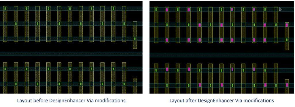
Figure 2. The Calibre DesignEnhancer flow enables design teams to quickly and easily back-annotate their IC design layouts for signoff analysis. Calibre DesignEnhancer leverages foundry-preferred Calibre design rule decks and Calibre connectivity data to ensure that all layout modifications are Calibre-clean and meet design rule check (DRC) constraints. Here’s an overview of the main use models and how each of them contributes to achieving PPA goals: Via insertion for IR drop mitigation How it works: The via insertion feature lets users identify critical nets and automatically maximizes vias on that net to reduce IR drop. Calibre’s complete understanding of the DRC rules enable superior results without introducing costly respins. Key processes: A “Via kit” includes all the complex via-related rules needed to ensure correct placement and compliance with DRC constraints through access to multilayer enclosure and extension rules, net type spacing, via count checks, coloring rules and other critical parameters. Benefits: The automated process enhances manufacturing robustness and reduces IR drop without resorting to manual placement. By prioritizing high-current nets, design teams optimize both runtime and resource usage (figure 3). Real usage of Calibre DesignEnhancer has shown that adding vias adding vias to power nets using the Via use model provided up to a 68% reduction in IR drop violations.
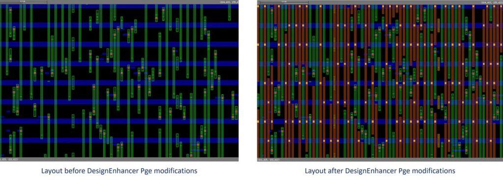
Figure 3. Automated via insertion using the Calibre DesignEnhancer Via use model maximizes the insertion of Calibre-clean sign-off quality vias. Parallel run lengths for enhanced electromigration resilience How it works: The tool identifies open tracks for additional metal and via insertion, creating parallel run lengths that reduce resistance on power grid lines to address both IR drop and EM. Key processes: Using the results of EMIR analysis, Calibre DesignEnhancer uses inserts Calibre-clean parallel metal and vias to reduce resistance. This targeted approach allows design teams to focus enhancements on areas most vulnerable to EM, rather than making blanket changes across the design. Benefits: Parallel runs reduce EMIR impact with minimal effect on timing. The process is efficient enough to run at the block or even chip level, making it viable for large-scale designs where EMIR issues could become significant bottlenecks (figure 4).
Figure 4. The Calibre DesignEnhancer Pge use model automatically inserts Calibre-clean metal and vias in open areas to help lower resistance on power grid structures. Advantages of design-stage layout modifications Adopting a tool like Calibre DesignEnhancer provides compelling business benefits that go beyond technical capabilities. Here’s how:
Achieving shift-left verification with Calibre confidence The shift-left methodology brings verification and optimization earlier in the design flow, allowing designers to tackle potential issues before they become costly problems at signoff. With Calibre DesignEnhancer, design teams can incorporate DRC constraints and foundry-preferred rules directly into layout modifications, ensuring that designs meet both electrical and physical verification requirements as early as possible, streamlining the path to successful tapeout. Adopting Calibre’s analysis-based layout modification solutions gives companies Calibre confidence that their designs are DRC-compliant and optimized designs, reducing the risks associated with IR drop, EM and physical signoff. Learn more about IC power management Design-stage layout modifications offer IC design teams and decision-makers an effective way to improve power management, streamline design cycles and reduce costs. By adopting a shift-left approach to power grid optimization, teams can effectively address power management challenges during implementation, rather than reacting to them at signoff. To learn more about how to transform your design flow and confidently achieve EMIR targets, download our full technical paper today — Calibre DesignEnhancer design-stage layout modification improves power management faster and earlier. Category: Siemens |
|
|
|||||
|
|
|||||
|
|||||


