


EDACafe Editorial Roberto Frazzoli
Roberto Frazzoli is a contributing editor to EDACafe. His interests as a technology journalist focus on the semiconductor ecosystem in all its aspects. Roberto started covering electronics in 1987. His weekly contribution to EDACafe started in early 2019. Special Report: Present and Future of the EDA Oligopoly – Part TwoApril 27th, 2023 by Roberto Frazzoli
Will the market dominance of EDA’s “big three” remain immune from the new factors that are impacting the semiconductor ecosystem? We tried to answer this question with the help of Laurie Balch (Pedestal Research), Harry Foster (Siemens EDA), David Kanter (MLCommons), KT Moore (Cadence), Wally Rhines (Cornami) In Part One of this special report we focused on the factors of stability that have contributed to the creation of the EDA oligopoly (Cadence, Siemens EDA and Synopsys, of course) and still underpin the incumbents’ market dominance: a certain degree of complementarity among the ‘big three’ product offerings, and the high cost incurred by customers if they want to switch from one EDA vendor to another. We also examined the overall performance of EDA solutions for IC/ASIC design through the findings of the 2022 Wilson Research Group Functional Verification Study, which shows – on average – a 24 percent rate of first silicon success and a 33 percent rate of project completion without schedule slips. Additionally, we discussed the attitude of the EDA industry towards benchmarking and open-source tools. In this second part of our report we will address some of the criticisms that have been raised against the EDA oligopoly and will consider some potential factors of change. We will do that, again, through interviews with EDA professionals (Harry Foster, Chief Scientist Verification at Siemens EDA; KT Moore, VP of corporate marketing at Cadence; Wally Rhines, CEO at Cornami and formerly CEO at Mentor Graphics for twenty-four years), an EDA market analyst (Laurie Balch, Research Director at Pedestal Research) and an executive from a benchmarking consortium (David Kanter, Executive Director at MLCommons). A different view on the EDA status quo: DARPA and the OpenRoad project Is the vendor oligopoly a positive or a negative thing for the EDA users? Over the past few years, DARPA (Defense Advanced Research Projects Agency) has often expressed opinions that are relevant for a discussion on this topic. In particular, the EDA theme has been addressed by Serge Leef when he was Program Manager of the DARPA’s Microsystems Technology Office. Other relevant concepts can be found in the OpenRoad project lead by Professor Andrew Kahng from UC San Diego, one of the open-source EDA initiatives supported by DARPA. Unfortunately, neither Serge Leef – who left DARPA last year – nor any other DARPA spokesperson, nor Professor Kahng could be reached for comments, so here we will refer to documents that are publicly available online. Read the rest of Special Report: Present and Future of the EDA Oligopoly – Part Two Special Report: Present and Future of the EDA Oligopoly – Part OneApril 25th, 2023 by Roberto Frazzoli
Will the market dominance of EDA’s “big three” remain immune from the new factors that are impacting the semiconductor ecosystem? We tried to answer this question with the help of Laurie Balch (Pedestal Research), Harry Foster (Siemens EDA), David Kanter (MLCommons), KT Moore (Cadence), Wally Rhines (Cornami) The global EDA market is notoriously dominated by just three U.S.-based major vendors: Cadence, Siemens EDA and Synopsys, of course. This status quo has been stable for decades; will it continue to be this stable in the future? Several new events and trends have recently started impacting the semiconductor ecosystem: US-China tensions, the AI boom, the growth of hyperscalers, massive subsidies supporting the construction of new fabs around the world etc. Will any of these new events have an impact on the EDA oligopoly? We tried to answer this question by interviewing EDA professionals (Harry Foster, Chief Scientist Verification at Siemens EDA; KT Moore, VP of corporate marketing at Cadence; Wally Rhines, CEO at Cornami and formerly CEO at Mentor Graphics for twenty-four years), an EDA market analyst (Laurie Balch, Research Director at Pedestal Research) and an executive from a benchmarking consortium (David Kanter, Executive Director at MLCommons, whose contribution will be featured in the next part of this report). In this first part, we will delve deeper into the factors of stability that have contributed to the creation of the oligopoly and still underpin the incumbents’ market dominance. Adding to the description of the status quo, we will also focus on the overall performance of EDA solutions, as well as on the attitude of the EDA industry towards benchmarking and open-source tools. The second part of our report will address some of the criticisms that have been raised against the EDA oligopoly and will consider some potential factors of change. Read the rest of Special Report: Present and Future of the EDA Oligopoly – Part One AI-based macro placement; open-use LLMs; new silicon-compatible materials for AI applicationsMarch 30th, 2023 by Roberto Frazzoli
Artificial intelligence is the common underlying theme for most of this week’s updates. Among them, Nvidia is in the news with an EDA research work, after last week announcement concerning its solution for computational lithography – the last software step before mask production. Nvidia research on AI-based macro placement At the recent ISPD (International Symposium on Physical Design), a group of Nvidia researchers presented a paper on AI-based macro placement. The paper proposes AutoDMP, a methodology that leverages DREAMPlace, a preexisting open-source GPU-accelerated placer, to place macros and standard cells concurrently in conjunction with automated parameter tuning using a multi-objective hyperparameter optimization technique. As a result, the team could generate high-quality predictable solutions, improving the macro placement quality of academic benchmarks compared to baseline results generated from academic and commercial tools. According to the Nvidia researchers, AutoDMP is also computationally efficient, optimizing a design with 2.7 million cells and 320 macros in three hours on a single Nvidia DGX Station A100. The key contributions of the work include using multi-objective Bayesian optimization to search the design space of macro placements, targeting three PPA proxy objectives post-place: wirelength, cell density, and congestion; using a two-level PPA evaluation scheme to manage the complexity of the search space; and enhancing the DREAMPlace placer. Open-source benchmarks used include Ariane, a single core Risc-V CPU; the MemPool Group and BlackParrot designs, many-core Risc-V CPUs with large amounts of on-chip SRAMs; and an NVDLA partition. A previous research work on AI-based macro placement, from Google, had been criticized for not providing enough publicly available data and for comparing the AI performance to an unspecified human expert’s performance. The new Nvidia work seems to be able to withstand these types of criticism, as it includes details on benchmarking and compares the AI performance with a commercial EDA tool, Cadence Innovus. The work’s source code is released on GitHub. Nvidia’s computational lithography software; Arm to reportedly raise prices; hardware Trojans; downscaling spintronicsMarch 23rd, 2023 by Roberto Frazzoli
Manufacturing-related innovations make up a large part of this week’s news roundup. Arm vs Risc-V is also a theme, with the open-source ISA gaining ground in China while Arm’s IP is reportedly set to become more expensive. Nvidia cuts processing time for computational lithography The new Nvidia cuLitho software library for computational lithography promises to slash the time and energy required to produce photomasks. Mask manufacturing at advanced nodes requires a vey complex compensation of the pattern distortions caused by the diffraction of light or EUV rays. Simplistically explained, the compensation is essentially obtained by transforming the design polygons into complex shapes, so that the combined effect of these shapes and diffraction will eventually result in the desired polygons being projected on the resist. This transformation – an example of computational lithography – is obviously carried out by software running on a processing platform. With large chips now containing several dozen billion transistors, foundries working on advanced nodes need large datacenters to perform computational lithography. As we learn from Jensen Huang’s keynote given at this year’s GTC event, TSMC is currently using a 40,000 CPU server farm for computational lithography, absorbing 35 megawatts. With cuLitho, and running all parts of the computational lithography process in parallel, the workload can be handled by just five hundred Nvidia DGX H100 GPU-based systems, reducing power to ‘just’ 5 megawatts. According to Nvidia, in the near term, fabs using cuLitho could produce each day 3-5x more photomasks using 9x less power than current configurations. A photomask that required two weeks can now be processed overnight. 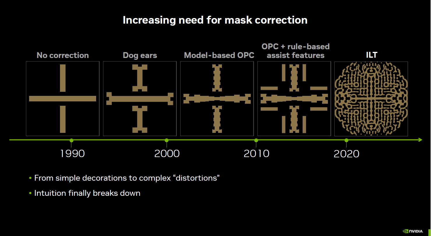 Source: Nvidia GTC. ILT stands for Inverse Lithography. Flexible NoCs; Tesla to cut SiC use; South Korea semi ambitions; GPT-4March 16th, 2023 by Roberto Frazzoli
The international race for semiconductor supremacy and the impact of electric vehicles on the SiC market are among the themes of this week’s news roundup. But first, some IP and EDA updates. IP and EDA updates: Signature IP, Defacto, Cadence New startup Signature IP aims to innovate the Networks-on-Chip IP scenario. As the company stated in a press release, the company’s purpose is to make it easy to design and configure the NoC backbone within a chip and benefit from the flexibility of exploring the design space before committing to an architecture. “There are few commercial NoC providers to choose from, and they are typically very restrictive in their architectures and commercial terms,” said CEO Purna Mohanty. “Our flexible iNoCulator NoC configuration tool enables customers to experiment with their SoC architecture and simulate it in real time so they can optimize it at the top level.” Offered as Software-as-a-Service, iNoCulator NoC Configurator can generate both coherent and non-coherent NoCs. It enables users to change the NoC topology, experiment with different configuration settings, and simulate the results to measure throughput and latency. Defacto has announced SoC Compiler 10.0, the new major release of its front-end design solution for large SoCs. Among new pre-synthesis design features, the ability to use both Accelera’s IP-XACT and RTL as input formats for internal and external IPs at different design steps; “ifdef” support to generate generic and configurable RTL code; a higher degree of automation in the management of design collaterals such as UPF and SDC jointly with RTL and IP-XACT; and Python native support. Read the rest of Flexible NoCs; Tesla to cut SiC use; South Korea semi ambitions; GPT-4 Ford re-enters the AV race; 2022 foundry results; Risc-V at European conferencesMarch 9th, 2023 by Roberto Frazzoli
The Netherlands’ government is reportedly planning new restrictions on exports of semiconductor technology. The restrictions will obviously impact ASML’s litho equipment, and – according to the report – will also affect DUV systems. More updates included in this week’s roundup concern automotive applications, foundry results, and upcoming European conferences. Automotive updates: Ford, imec, proteanTecs Ford Motor Company has established Latitude AI, a wholly owned subsidiary focused on developing automated driving systems. The move comes just a few months after the company shut down Argo AI, a self-driving technology unit that Ford ran in collaboration with Volkswagen. Latitude employs about 550 employees formerly of Argo AI and is headquartered in Pittsburgh – with additional engineering hubs in Dearborn, Michigan, and Palo Alto, California. Belgian research center Imec has developed a digitally calibrated charge-pump phase-locked loop that can generate high-quality frequency-modulated continuous-wave signals for mmWave radars at low power consumption. The novel PLL is a critical building block for future short-range automotive (in-cabin and out-of-cabin) and industrial radar applications. Read the rest of Ford re-enters the AV race; 2022 foundry results; Risc-V at European conferences IP and VIP updates; new fabs; CHIPS Act applicant requirements; Intel strategies; Keysight acquires CliosoftMarch 2nd, 2023 by Roberto Frazzoli
Catching up on some of the news from the last three weeks or so, let’s start with a Silicon Valley update: Tesla global engineering headquarters are moving to Palo Alto. The company is reportedly taking over the lease for the office space previously occupied by Hewlett-Packard. More news this week concern new fabs around the world and the U.S. CHIPS Act. But first, some IP and VIP updates. IP, VIP and validation updates: Arteris, Avery, Cadence, Imperas Arteris has launched its FlexNoC 5 physically aware network-on-chip IP, which enables SoC designers to incorporate physical constraint management across power, performance and area (PPA). According to the company, this technology enables up to 5X faster physical convergence over manual refinements with fewer iterations from the layout team. The resulting physically optimized NoC IP instance is ready for output to physical synthesis and place and route for implementation. Arteris has also formed a partnership with Risc-V IP vendor SiFive, to help speed up edge AI product development. As a result of this collaboration, SiFive has developed the 22G1 X280 Customer Reference Platform, incorporating a SiFive X280 processor IP and an Arteris Ncore cache coherent interconnect IP. Avery Design Systems has announced a new validation suite supporting the Compute Express Link (CXL) open industry-standard interconnect. It enables system interoperability, validation and performance benchmarking of systems targeting the full range of versions of the CXL standard. According to the company, sharing the same validation suite across pre- and post-silicon enables hardware and software development teams to start system integration and validation extremely early in the project while still working with Verilog RTL simulation and emulation. Special report: 2023 SEMI Industry Strategy Symposium EuropeFebruary 23rd, 2023 by Roberto Frazzoli
European company executives and analysts got together to discuss old continent’s strengths and weaknesses, aiming to make the most of the subsidies that the EU Chips Act will provide to the European semiconductor ecosystem Necessary but not sufficient: this is how the EU Chips Act – the subsidy plan recently passed by the European Union to support Europe’s semiconductor industry – is perceived by many of the company executives and analysts convened in Vienna on February 15th and 16th for the 2023 edition of the annual SEMI European Industry Strategy Symposium. Organized by SEMI Europe – regional office of the global industry association representing the electronics manufacturing and design supply chain, the event attracted over two hundred attendees and offered valuable insights on a number of themes that are expected to impact not just the old continent, but also its geopolitical and technological partners in America and Asia. The two-day symposium saw the participation of over thirty speakers and offered three panel discussions. 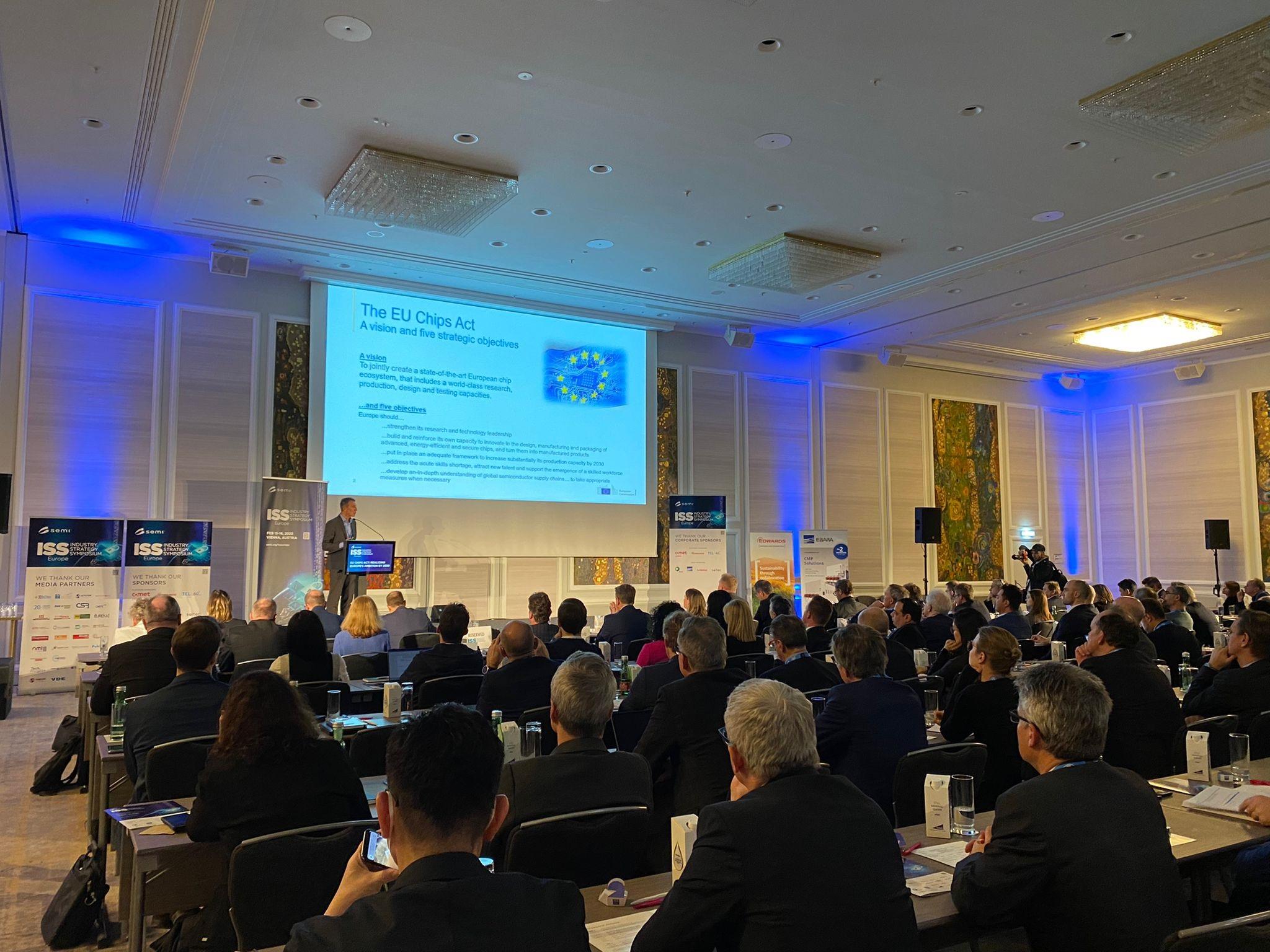 Credit: SEMI Europe In this article we will briefly summarize some of the symposium content – starting with the welcome remarks from Laith Altimime, President of SEMI Europe. Altimine outlined SEMI Europe’s agenda to make the European Chips Act a success: focus across the whole manufacturing ecosystem (materials, chemicals, gases, design, equipment, manufacturing and RTOs) to support supply chain resilience and industry growth; pursue stakeholders’ collaboration to achieve industry sustainability goals, considering that the industry has the urgent need of introducing smart and green manufacturing solutions and pave the way to net zero; support Europe’s talent pipeline transformation with concrete funds and investments, to close the talent gap and cultivate the workforce of tomorrow; foster industry participation – through the European Semiconductor Board – to ensure expertise-based decision making and inclusive governance; leverage the European “chip diplomacy”, going forward as one on export control, investments, supply chain as well as innovation and R&D. Read the rest of Special report: 2023 SEMI Industry Strategy Symposium Europe Benefits of AI-based EDA; static linting for FPGAs; ESD diode Spice model; open-source eFPGA dev suite; PCB SI/PI analysisFebruary 9th, 2023 by Roberto Frazzoli
A couple of ‘geopolitical’ updates. General Motors and GlobalFoundries have announced a strategic, long-term agreement establishing a dedicated capacity corridor exclusively for GM’s chip supply. Through this first-of-its-kind agreement, GlobalFoundries will manufacture for GM’s key chip suppliers at GF’s advanced semiconductor facility in upstate New York, bringing a critical process to the U.S. Thomas Caulfield, president and CEO of GlobalFoundries, said that GF will expand its production capabilities exclusively for GM’s supply chain. And the U.S. government is reportedly poised to extend restrictions to American investments that are used to finance the development of advanced technologies in China. According to the report, the executive order would most likely prohibit outright investments in some sensitive areas, like quantum computing, advanced semiconductors and certain artificial intelligence capabilities with military or surveillance applications. STMicroelectronics and SK Hynix unveil results achieved using Synopsys DSO.ai Synopsys’ AI-based DSO.ai design system has reached the mark of 100 commercial tape-outs. The announcement includes quotes from two important Synopsys customers, unveiling the results they obtained. STMicroelectronics, which used Synopsys DSO.ai on Microsoft Azure cloud, increased PPA exploration productivity by more than 3x, allowing fast implementation of a new Arm core, while exceeding power, performance and area goals. SK hynix cited a recent project where DSO.ai delivered a 15% cell area reduction and a 5% die shrink. New Siemens verification solution; Intel and AMD 2022 results; Intel Pathfinder discontinued; U.S.-India partnershipFebruary 2nd, 2023 by Roberto Frazzoli
Among the latest updates on U.S.-China tensions, the Biden administration has reportedly stopped approving licenses for U.S. companies to export most items to Huawei; and Netherlands and Japan have reportedly agreed to the U.S. request of restricting exports of chipmaking tools (from ASML, Tokyo Electron etc.) to China. Let’s now move to other news, starting with some EDA updates. Siemens aims to accelerate verification closure Verification productivity continues to be a hot topic for the EDA industry. Siemens has just introduced Questa Verification IQ software – a solution that leverages big data and AI to accelerate verification closure. As explained in a press release, Questa Verification IQ is tightly integrated with Siemens’ Polarion Requirements software to deliver a platform that automatically captures all data from every engine run across the life of a project, helping users manage requirements, coding, testing and release management across the design and verification process. According to Siemens, this combination provides a digital thread optimized for functional safety compliance tasks, providing a traceable solution from requirements down to verification results and implementation. Questa Verification IQ unifies coverage data from the formal and simulation engines within Siemens’ Questa platform, OneSpin software, Symphony platform for analog and mixed-signal simulation, as well as Siemens’ Veloce hardware for emulation and prototyping. The machine learning functionality in Questa Verification IQ then analyzes the data to predict patterns and holes, identify root causes, and prescribe solutions to potential issues. Questa Verification IQ is implemented in a web-based application framework. |
|
|
|||||
|
|
|||||
|
|||||


 Animation, 3D Art and 3D Models")