


EDACafe Editorial Roberto Frazzoli
Roberto Frazzoli is a contributing editor to EDACafe. His interests as a technology journalist focus on the semiconductor ecosystem in all its aspects. Roberto started covering electronics in 1987. His weekly contribution to EDACafe started in early 2019. FTC opposes Nvidia-Arm deal; Mobileye to go public; Renesas enters the FPGA market; Toshiba to split in three; acquisition updatesDecember 10th, 2021 by Roberto Frazzoli
Catching up on some of the news from the last thirty days or so, let’s start with some market data: according to market research firm Omdia, in the third quarter of 2021 the semiconductor market surpassed $150 billion and Samsung Electronics overtook Intel as number one semiconductor firm in the revenue ranking, on the strength of its memory business. Moving to some fab updates, Samsung has officially confirmed it would build a new semiconductor manufacturing facility in Taylor, Texas, with an estimated $17 billion investment. TSMC, for its part, will build a specialty technology fab in Kumamoto, Japan, with Sony Semiconductor Solutions participating as a minority shareholder. 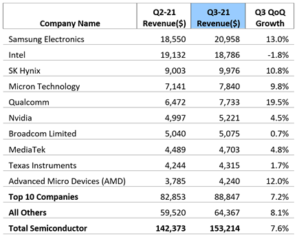 Credit: Omdia FTC sues to block Nvidia’s acquisition of Arm As widely reported by many media outlets, the United States’ Federal Trade Commission filed a law enforcement action to block Nvidia’s acquisition of Arm, “to preserve competition in markets for computer chips used in datacenters and in automotive advanced driver assistance systems.” The administrative trial is scheduled to begin on August 9, 2022. The FTC’s position about the “anticompetitive effects” of the proposed acquisition is described in detail in this twenty-four-page document. The Mirabilis Design approach to system-level architecture explorationDecember 1st, 2021 by Roberto Frazzoli
Achieving 5x battery life without any hardware changes: according to Deepak Shankar, Mirabilis Design’s founder, this is an example of the benefits that can be obtained through his company’s system-level architecture exploration solution, based on the VisualSim IP libraries System-level architecture exploration is an increasingly important task for designers, especially when it comes to optimizing power or performance for complex SoC designs. Software company Mirabilis Design (Sunnyvale, CA) has chosen to address this specific area, through a system-level simulation platform – its flagship product VisualSim Architect – that employs IP libraries built in-house. In the last year and a half, the company has seen almost a 6x increase in revenue and almost a 15x jump in the number of customers (source: Mirabilis Design data), partly owing to the new remote collaboration needs brought about by the Covid-19 pandemic. Deepak Shankar, founder and Vice President of Technology at Mirabilis Design, has reiterated the key concepts of his company’s approach in the video interview he has recently given to EDACafe’s Sanjay Gangal. For this article, he has also answered a few additional questions.
Read the rest of The Mirabilis Design approach to system-level architecture exploration A quick look at the 2021 Linley Fall Processor ConferenceNovember 18th, 2021 by Roberto Frazzoli
This week EDACafe takes a quick look at the 2021 edition of the Linley Fall Processor Conference, organized by technology analysis firm The Linley Group at a physical venue in Santa Clara, CA, and followed by a virtual event. Besides updates on deep learning accelerators, the conference also covered ‘conventional’ processing solutions and some other types of IP. This article will only provide a general overview of the event; full content can be accessed from the conference website, downloading the proceedings (presentations slides) for free. AI trends: bigger training workloads, segmentation of the edge-AI market In his opening keynote, Linley Group’s Principal Analyst Linley Gwennap reiterated the key concepts from last Spring processor conference, adding updates on the recent AI trends. Among them, the size of NLP models keeps growing: Google’s Switch Transformer has 1.6 trillion parameters. To train ever-larger neural networks, Cerebras and Tesla are using wafer-scale technology and other innovations. In the datacenter, Nvidia is finding tougher competition from Qualcomm AI 100 and forthcoming Intel Ponte Vecchio. According to Gwennap, Nvidia still leads in performance, but not in efficiency. As for edge-AI, this market is fragmenting into high-end chips for camera-based systems and low-power chips for simple sensors. The conference also saw the participation of TechInsights – the Canadian reverse engineering firm that has recently acquired The Linley Group – with a presentation on the performance gap between CPU and main memory. Among other findings, TechInsights analysts concluded that SRAM cell size scaling trend is getting worse than Logic Standard Cell because SRAM cell does not have DTCO (Design Technology Co-Optimization) scaling options. Read the rest of A quick look at the 2021 Linley Fall Processor Conference Latest release of Ansys HFSS 3D Components adds a new model delivery mechanismNovember 9th, 2021 by Roberto Frazzoli
Ansys’ Matt Commens explains the new function and recaps the key features of this collaboration tool, which enables designers of high frequency systems to use accurate 3D component models specifically developed for the HFSS simulation engine The latest Ansys release (2021 R2) includes updates to HFSS 3D Components, a tool that enables what the company calls “electromagnetic simulation collaboration” between component vendors and system integrators through the use of 3D component models specifically developed for HFSS (Ansys’ 3D high frequency electromagnetic simulation software). Matt Commens, Principal Product Manager for HFSS at Ansys, has described the key features and new functions of HFSS 3D Components in the video interview he has recently given to EDACafe’s Sanjay Gangal; in addition to that, we have asked Matt a few more questions on some specific aspects.
Read the rest of Latest release of Ansys HFSS 3D Components adds a new model delivery mechanism AV market consolidation; Indy AV race; solid-state batteries; acquisitionsNovember 1st, 2021 by Roberto Frazzoli
Global scrutiny of the Nvidia-Arm deal continues: adding to a list of other authorities, European Union regulators have reportedly opened an investigation over concerns of limited competition. The EU Commission said Nvidia had offered concessions to address preliminary concerns, but that they weren’t enough. A decision from European regulators is expected within March 15. As for the other news updates this week, several of them concern autonomous vehicles – including two acquisitions of radar specialist companies. Autonomous driving tech market is consolidating According to market intelligence firm CB Insights, a few key players are emerging in autonomous driving technology, and the market is consolidating around major companies like Waymo and Aurora. Every round backed by top venture capital firms in the AV market over the last two years has been Series C or later. This indicates that – as the AV market consolidates – the top VCs monitored by CB Insights “are focusing on the winners, seeing stronger potential for leading self-driving developers rather than early-stage companies.” Another sign of consolidation is the move from many deals to just a few big ones: total funding to autonomous driving companies spiked in 2018, but “since then, deal count has declined significantly as total funding continues to rise.” The majority of the funding by top VCs in AVs over the last two years “has come from just two mega-rounds ($2.25B in 2020 and $2.5B in 2021) to Waymo.” According to CB Insights, the top venture capital firms are now backing companies working on simulation and training, developing the full self-driving stack, enhancing mapping and localization, and more. “Total equity funding to the space has already eclipsed $12B in 2021, up more than 50% from all of 2020,” the analysts elaborated. The selected top VCs monitored by CB Insights “have participated in a record-breaking $3.85B of total funding to autonomous driving companies so far in 2021, with the total projected to be above $5.1B by year end if the trend continues.”  “Smart Money” refers to a group of top VCs as defined by CB Insights. Read the rest of AV market consolidation; Indy AV race; solid-state batteries; acquisitions TSMC and Samsung Foundry roadmaps; new Alibaba processors; Arm Virtual Hardware for IoTOctober 25th, 2021 by Roberto Frazzoli
Chips built using 2-nanometer processes will enter volume production in 2025; this, at least, is what we can expect based on the roadmap updates recently provided by both Samsung Foundry and TSMC. For the 2-nanometer node, the South Korean company will adopt its version of the gate-all-around transistor architecture; TSMC is also considering GAA, but has not committed to it yet. More news this week include a 60-billion transistor chip from Alibaba, and a multi-pronged Arm initiative meant to boost the IoT market. But first, a couple of EDA updates. Ansys adds a charging/discharging simulation solution Ansys has added EMA3D Charge to its simulation solution portfolio. Developed by Colorado-based Electro Magnetic Applications company, EMA3D Charge enhances predictive accuracy for charging and discharging events that can have an impact on safety for a wide range of electric/electronics products. Leveraging Ansys SpaceClaim, the solution combines CAD import, design and simplification, simulation setup and meshing, and result generalization and visualization into one solver technology. According to Ansys, EMA3D Charge fills a need in a marketplace in which no other simulation product exists, providing a unified end-to-end workflow. Cadence to speed up ISO 26262 and IEC 61508 certification Cadence has announced the Cadence Safety Solution, a new offering featuring integrated analog and digital safety flows and engines for faster ISO 26262 and IEC 61508 certification. Targeting safety-critical applications – such as automotive and aerospace – the solution includes a new failure modes, effects, and diagnostic analysis (FMEDA) offering called the Cadence Midas Safety Platform, allowing to perform FMEDA-driven analog and digital verification of safety-critical semiconductors. Discovering Cadence Integrity 3D-IC platformOctober 18th, 2021 by Roberto Frazzoli
Cadence’s Vinay Patwardhan explains how designers can tackle the challenges posed by 3D ICs using the new solution recently announced by the company Placing multiple chips in a single package – either in a 2.5D or in a 3D fashion – is emerging as a viable solution to continue advancing IC performance and functionalities using the currently available process nodes, while keeping die size within lithography reticle limits. However, a package containing two or more dies can be considered as a new type of system, posing new system-level challenges. Existing EDA tools – even the most advanced ones – are mostly meant to address the challenges posed by a single chip and its package; for this reason, the EDA industry is now coming up with new solutions specifically addressing the needs of 2.5D and 3D ICs. Cadence, in particular, has recently announced a new platform called “Integrity 3D-IC”, which it describes as the “industry’s first comprehensive 3D-IC platform for multi-chiplet design and advanced packaging”. To know more about this solution, EDACAfe’s Sanjay Gangal has conducted a video interview with Vinay Patwardhan, Product Management and Group Director, Digital and Signoff Group at Cadence Design Systems.
Read the rest of Discovering Cadence Integrity 3D-IC platform GloFo to go public; Intel’s Risc-V-based soft processor; Chinese investments in Q3; pixel-shift for smartphonesOctober 13th, 2021 by Roberto Frazzoli
Geopolitical tensions made headlines over the past few days, with Chinese President Xi Jinping in his recent speech reportedly vowing to pursue reunification with Taiwan. Needless to say, this news is also relevant to the semiconductor industry as Taiwan is homeland of the world’s largest foundry. Let’s now move to this week’s updates, which include a quick look at some companies based in mainland China attracting significant investments. GlobalFoundries to go public GlobalFoundries has publicly filed a registration statement with the U.S. Securities and Exchange Commission (the SEC) relating to the proposed initial public offering of its ordinary shares. GF has applied to list on the Nasdaq Global Select Market under the ticker symbol GFS. Intel offers a Risc-V-based soft processor for its FPGAs The new generation of Nios, the soft processor for Intel FPGAs, is based on the open-source Risc-V Instruction Set Architecture. Called Nios V, the family currently includes a micro controller – Nios V/m – based on Risc-V: RV32IA, with atomic extensions, 5-stage pipeline, and AXI4 interfaces. Future releases will include a general-purpose processor, an application-class processor, and a Linux-capable processor. Benefits cited by Intel include the open-source ecosystem – toolchains, debuggers, real-time operating system – and performance improvements over the Nios II/e processor. The new Nios V soft processor is available in the Intel Quartus Prime Pro Edition Software starting with version 21.3. New MathWorks release; Arteris IP to go public; compact Risc-V IP; Arm-based servers for AI workloads; new Loihi chipOctober 6th, 2021 by Roberto Frazzoli
Catching up on some of the news from the last couple of weeks or so, let’s briefly recall that European Union politicians have started discussing about a plan to support the semiconductor industry in the Old Continent. The President of the European Commission, Ursula von der Leyen, has recently preannounced a European Chips Act. “We need to link together our world-class research, design and testing capacities,” she said in her recent State of the Union speech. “We need to coordinate EU and national investment along the value chain. The aim is to jointly create a state-of-the-art European chip ecosystem, including production. That ensures our security of supply and will develop new markets for ground-breaking European tech. (…) We are world leaders. So let’s be bold again, this time with semi-conductors.” Additional details on the upcoming European Chips Act have been provided by European Commissioner Thierry Breton in this blog post, quoting Imec, CEA-Leti and Fraunhofer as key European assets. “I believe that we should explore setting up a dedicated European Semiconductor Fund,” he wrote. “With the European Chips Act, our tech sovereignty is within reach.”  Copyright European Union, 2021. Photographer: Christophe Licoppe EDA/IP updates: Cadence, MathWorks, Arteris IP, Bluespec, Sigasi The new Cadence Helium Virtual and Hybrid Studio is a platform that accelerates the creation of virtual and hybrid prototypes of complex systems. According to Cadence, Helium Studio makes verification with a virtual or hybrid model of the SoC orders of magnitude faster than verification with a pure RTL model, and it also enables early software bring-up before the RTL is available. Natively integrated with the Cadence verification engines – including Palladium Z2, Protium X2 and Xcelium – the new Helium Studio accelerates system development by verifying embedded software/firmware on pure virtual and hybrid configurations even when the RTL is not ready. Siemens enters the IC power integrity analysis market with a solution for analog, digital and mixed-signal designs of any sizeSeptember 28th, 2021 by Roberto Frazzoli
Called mPower, the new software fills an important gap in the EDA market, says Siemens’ Joe Davis Smaller process geometries make electromigration (EM) and voltage drop (IR) analysis more important than ever for new chip designs, as interconnects and material layers get thinner and thinner. At the same time, smaller geometries mean skyrocketing transistor counts, making detailed EM/IR analysis of a full design a daunting task. On top of that, the growth of sensor-based applications leads to larger analog blocks, where the techniques used in digital blocks to simplify EM/IR analysis are not applicable. Is the EDA industry keeping pace with the ever-harder requirements of power integrity analysis? According to Siemens, until yesterday the answer was no – and this resulted in some critical pain points. “The largest, most complex analog systems are often sent to manufacturing without a detailed EM/IR analysis; simplifications, subsetting the design, less accurate simulators and other ad hoc methods are used as approximations; lack of detailed EM and IR analysis for large-scale analog circuits puts the whole system at risk,” Siemens maintains in a document on this topic. Identifying those pain points as a market opportunity, Siemens is now introducing its new mPower power integrity software for analog, digital and mixed-signal IC designs. Let’s take a closer look at mPower with the help of Joe Davis – Senior Director at Calibre Interfaces, EM/IR Product Management at Siemens – who recently gave a video interview on this topic to Sanjay Gangal from EDACafe. |
|
|
|||||
|
|
|||||
|
|||||


 Animation, 3D Art and 3D Models")