Let’s start by briefly mentioning two U.S. CHIPS Act updates. Polar Semiconductor will receive up to $123 million in direct funding to expand and modernize the company’s manufacturing facility in Bloomington, Minnesota. The investment is expected to nearly double the U.S. production capacity of sensor and power chips. The U.S. government has also launched the National Semiconductor Technology Center’s (NSTC) Workforce Center of Excellence (WCoE), with an expected $250 million investment over ten years, to support education programs that address key skills and workforce gaps in the semiconductor industry. The first cohort of awardees consists of the following organizations: American Federation of Teachers Educational Foundation, Idaho Technology Council, Maricopa County Community College District, Rochester Institute of Technology, Texas A&M University, University of California Los Angeles, University of Illinois Urbana-Champaign.
Latest EDA updates from TSMC OIP Forum North America
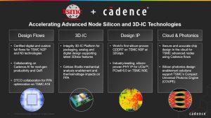
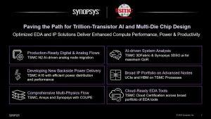
On occasion of TSMC OIP Forum North America, held in Santa Clara on September 25, the major EDA vendors announced their latest tool certifications and new collaborations with the Taiwanese foundry. In general, tool certifications mainly concern TSMC’s N2 process, and areas of collaboration include backside power delivery for the foundry’s A16 process, 3D packaging, multiphysics simulation, IP, cloud-based EDA and more. Here are the announcements from Ansys, Cadence, Siemens and Synopsys. The agenda of the TSMC event, with abstracts of the presentations, can be found here. Below, two charts summarizing the news from Cadence and Synopsys.


