


EDACafe Editorial Roberto Frazzoli
Roberto Frazzoli is a contributing editor to EDACafe. His interests as a technology journalist focus on the semiconductor ecosystem in all its aspects. Roberto started covering electronics in 1987. His weekly contribution to EDACafe started in early 2019. New US GlobalWafers fabs; new AI robotic model; SoftBank acquires Graphcore; semiconductor-specialized LLMJuly 18th, 2024 by Roberto Frazzoli
Not surprisingly, several interesting updates this week regard artificial intelligence in one way or another. Among them, the news about robotic startup Skild attracts the attention on the marriage between AI and robotics, a promising perspective also from the point of view of the study of living beings. So far, AI has achieved incredible language-centric performance: AI can even emulate the skills of a semiconductor expert, just see the news about SemiKong below. But throughout evolution, language is just the latest addition to a range of other key functions that are still difficult if not impossible to artificially replicate. Motion control is definitely one of those key functions: still today, we have no idea of how we could build a robot performing like a playing kitten – a small mammal, very far away from human beings in the evolution tree. In nature, there is no such thing as a language skill without a body, and there has to be a reason for that. So focusing on motion control sounds like approaching the problem from the right side. GlobalWafers to get CHIPS act funding The U.S. Department of Commerce plans to provide up to $400 million under the CHIPS and Science Act to Taiwan-headquartered GlobalWafers to build and expand facilities in Sherman, Texas (to establish the first 300mm silicon wafer manufacturing facility for advanced chips in the United States) and in St. Peters, Missouri (to establish a new facility to produce 300mm silicon-on-insulator wafers). Further, GlobalWafers plans to convert a portion of its existing silicon epitaxy wafer manufacturing facility in Sherman, Texas to silicon carbide epitaxy wafer manufacturing, producing 150mm and 200mm SiC epitaxy wafers.
New funding for DreamBig San Jose-based DreamBig Semiconductor has announced a $75 million equity funding round. These funds will bolster the development and commercialization of products built on DreamBig’s Chiplet Hub and Platform Chiplets, targeted at AI and data center infrastructure. The Chiplet Hub architecture offers an alternative to the usual way of assembling a multi-die device that includes processor cores, HBMs and I/Os. The differences between the two approaches are described in this video. Micron’s MRDIMM Micron Technology is now sampling its “multiplexed rank dual inline memory modules” (MRDIMMs), addressing the expanding demands of data center workloads. According to the company, MRDIMMs provide the following advantages over RDIMMs: up to 39% increase in effective memory bandwidth; greater than 15% better bus efficiency; up to 40% latency improvements. 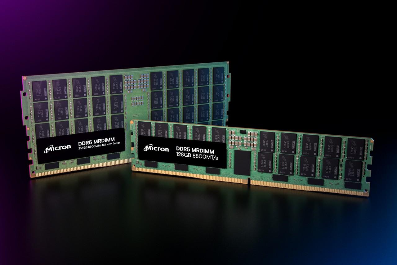 Micron’s MRDIMM. Credit: Micron Technology Skild AI’s robotic model Skild AI has officially come out of stealth mode, announcing that it has raised $300 million in Series A funding, which values the company at $1.5 billion. The round was led by Lightspeed Venture Partners, Coatue, SoftBank Group, and Jeff Bezos (through Bezos Expeditions), with participation from Felicis Ventures, Sequoia, Menlo Ventures, General Catalyst, CRV, SV Angel, Carnegie Mellon University, and the Amazon Industrial Innovation Fund & the Alexa Fund. “As opposed to vertically designed robots that are built for specific applications or only deployed in isolated or constrained environments, our model serves as a general-purpose brain,” the company stated in a blog post. “It has demonstrated unparalleled generalization and emergent capabilities across a diverse embodiment of robots, scenarios and tasks, including manipulation, locomotion and navigation.” To achieve this, “Our foundation model is trained on an unparalleled scale of data, representing a breakthrough in the robotics data barrier.” In Skild’s view, “our model will enable the use of low-cost robots across a broad range of industries and applications.” According to investor Sequoia Capital, “a GPT-3 moment is coming to the world of robotics.” 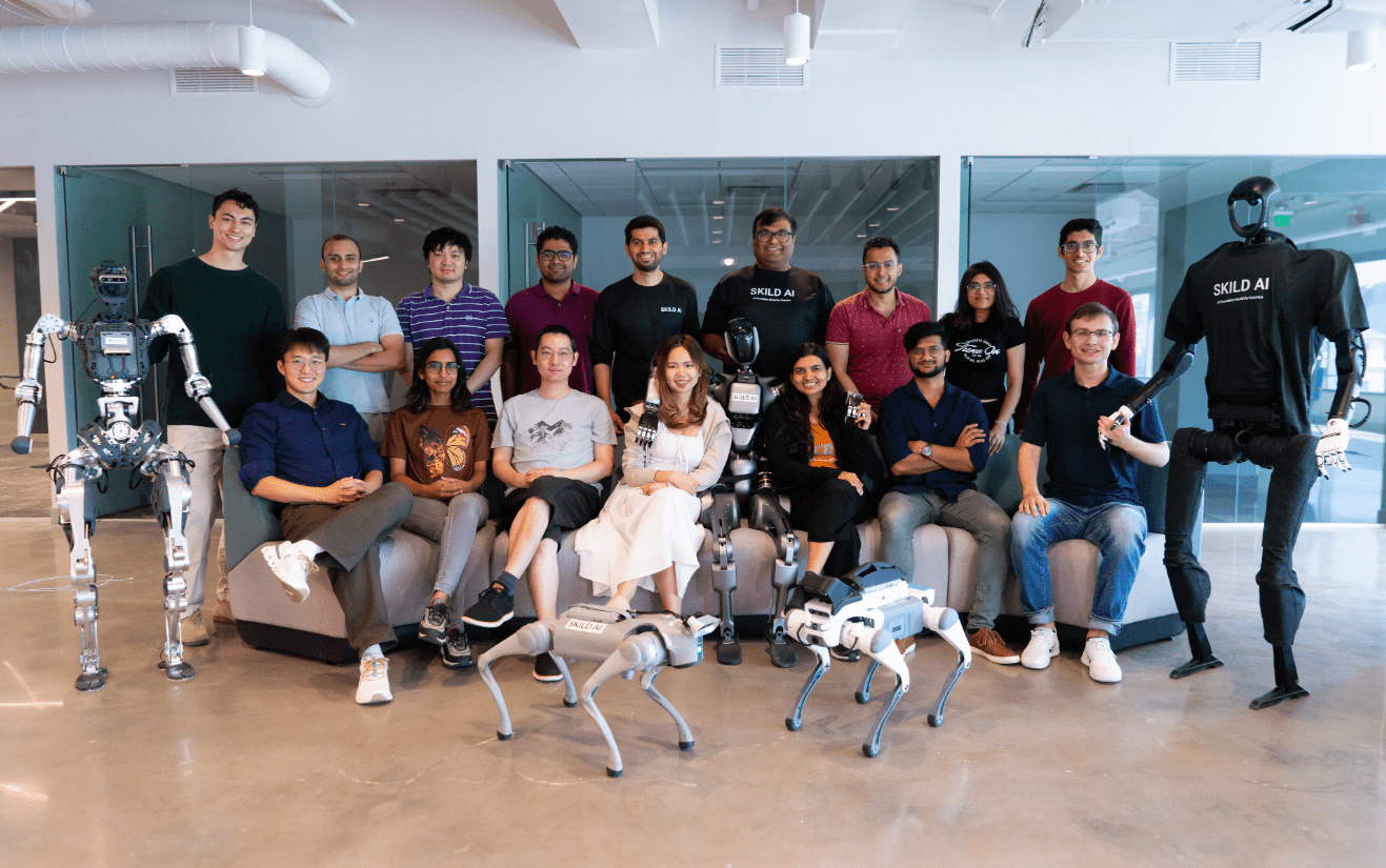 The Skild AI team. Credit: Skild AI A Large Language Model designed specifically for the semiconductor industry Launched by Aitomatic and supported by Meta, Tokyo Electron, and FPT Software, SemiKong is “the world’s first open-source AI Large Language Model designed specifically for the semiconductor industry.” To test the tool’s capabilities, EDACafe submitted to SemiKong the following question: “Is High-NA EUV better than double patterning with standard EUV?” And here’s the answer automatically generated by SemiKong: “High-NA (Numerical Aperture) Extreme Ultraviolet Lithography (EUVL) and double patterning with standard EUVL are two different approaches to advanced lithography in semiconductor manufacturing. To compare their performance, we need to consider factors such as resolution, overlay accuracy, mask complexity, and cost. High-NA EUVL is a technique that uses a higher numerical aperture objective lens in the EUV lithography system to achieve a smaller focus spot size, resulting in better resolution and reduced printing errors. This allows for the creation of smaller features and denser patterns on the wafer surface, which can lead to increased transistor density and improved overall device performance. Double patterning with standard EUVL, on the other hand, is an approach that employs a combination of multiple exposures and pattern multiplication to create smaller features on the wafer surface. This technique can help maintain the same resolution as traditional EUVL while enabling the creation of denser patterns. When comparing the two approaches, it’s essential to consider the specific application and requirements of the semiconductor manufacturing process. In general, High-NA EUVL has the potential to offer better resolution and overlay accuracy than double patterning with standard EUVL, which can result in improved device performance and reduced printing errors. However, High-NA EUVL may also come with higher costs due to the need for more complex optics and mask design. In conclusion, High-NA EUVL has the potential to be better than double patterning with standard EUVL in terms of resolution and overlay accuracy, but the decision between the two approaches ultimately depends on the specific requirements and constraints of the semiconductor manufacturing process, as well as the tradeoffs between cost, complexity, and performance.” Source: SemiKong. Acquisitions AI chip developer Graphcore has been acquired by SoftBank Group. Under the deal, Graphcore becomes a wholly owned subsidiary of SoftBank and will continue to operate under the Graphcore name. The company’s headquarters remain in Bristol, with offices in Cambridge, London, Gdansk and Hsinchu. Samsung Electronics has signed an agreement to acquire Oxford Semantic Technologies, a spin out of the University of Oxford (UK) specializing in knowledge graph technology. According to Samsung, this technology will be applicable across all of Samsung’s products, extending beyond just mobile devices to televisions and home appliances. L&T Semiconductor Technologies, a wholly owned subsidiary of the Indian construction giant Larsen & Toubro, is reportedly acquiring a 100% stake in SoC design startup SiliConch Systems. Chip war updates Google and Microsoft’s cloud divisions are reportedly offering Chinese companies access to Nvidia’s AI chips by providing data center services in locations outside China. According to the report, Microsoft in particular offers server rental services, including those with Nvidia’s A100 and H100 chips, to Chinese customers through data centers outside China. An article from ChinaTalk discusses the fact that, late last month, developers in China lost API access to OpenAI’s services. According to the author, API access is one of the less-discussed vectors of export control, and Chinese developers can go around this restriction in a number of ways, such as using a VPN while making API calls. |
|
|
|||||
|
|
|||||
|
|||||


 Animation, 3D Art and 3D Models")