


Not surprisingly, Samsung Foundry’s recent event confirmed at least two of the trends also recently highlighted by TSMC: the adoption of backside power delivery and the development of technologies that make it possible to place an electric chip and an optical chip in the same package. A frivolous remark on process naming: contrary to Intel Foundry and TSMC, Samsung has not switched to the Angstrom unit and prefers using tenths of a nanometer, with a point (SF1.4). Probably the most surprising announcement this week comes from a Finnish startup, claiming that it can boosts the performance of any existing multicore CPU up to 100-fold. An obvious question comes to mind: why haven’t the leading CPU vendors of the world come up with a similar solution yet? We’ll try to find out as soon as we can.
Roadmap updates from the U.S. Samsung Foundry Forum
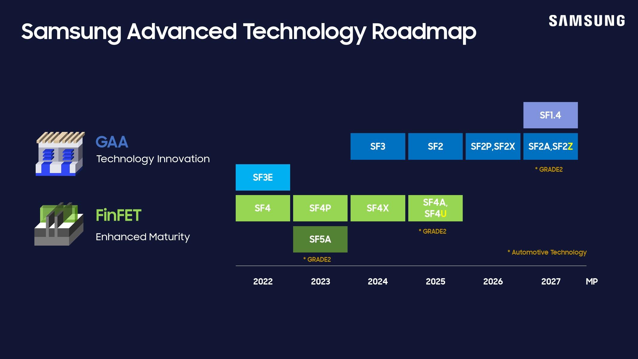
At the recent U.S. Samsung Foundry Forum, the South Korean company announced two new process nodes, SF2Z and SF4U. The company’s latest 2-nanometer process, SF2Z, incorporates optimized backside power delivery network (BSPDN) technology, enhancing PPA compared to SF2 and reducing voltage drop. Mass production of SF2Z is slated for 2027. SF4U is described as a “high-value” 4-nanometer variant that offers PPA improvements by incorporating optical shrink, with mass production scheduled for 2025. Samsung also reaffirmed that its preparations for SF1.4 (1.4-nanometer) are progressing smoothly, with performance and yield targets on track for mass production in 2027. The company emphasized the maturity of its GAA (gate-all-around) technology, which will be used to mass produce Samsung’s second-generation 3-nanometer process (SF3) in the second half of this year and the upcoming 2-nanometer process. Another highlight was the unveiling of Samsung AI Solutions, a turnkey AI platform resulting from collaborative efforts across the company’s Foundry, Memory and Advanced Package businesses, enabling a 20% improvement in total turnaround time. The company is also planning to introduce integrated, co-packaged optics (CPO) technology.
Credit: Samsung Foundry


 Animation, 3D Art and 3D Models")