Artificial Intelligence keeps creating “circles” – that is, producing consequences that feedback on AI itself, further amplifying its impact. Besides the well-known chip performance “virtuous circle” (powerful processors enabling AI, and AI enabling even more powerful processors), another circle is looming – virtuous or vicious, depending on the point of view. It can be described as follows: chip fabs capacity enables the construction of large datacenters, and the success of AI applications fueled by large datacenters generates the demand for even larger fab capacity. Clearly, this insatiable hunger for GPUs is “virtuous” from the point of view of semiconductor sales, but can be considered “vicious” from an energy consumption standpoint. According to a CB Insights estimate, in 2024 three million operational H100 Nvidia chips – in datacenters around the world – will collectively consume almost 14 GWh, more than the whole Guatemala state (13 GWh).
Sam Altman reportedly looking to spur the construction of new fabs
According to two press reports (here and here), OpenAI’s CEO Sam Altman is trying to launch a network of new fabs to ensure his company an abundant supply of GPUs and reduce its reliance on Nvidia. Reportedly, Altman has been discussing the project with investors from United Arab Emirates and Japan’s SoftBank Group – as well as with potential foundry partners like TSMC, Intel and Samsung. OpenAI would be the new fabs’ primary customer. “Big tech” companies are the biggest buyers of Nvidia’s H100 GPUs. In a Thread post (quoted by Reuters), Mark Zuckerberg recently wrote “We’re building a massive amount of infrastructure. At the end of this year, we’ll have ~350k Nvidia H100s — and overall ~600k H100 equivalents of compute if you include other GPUs”.
Is the $35 billion deal going to change the EDA oligopoly? Is the need for better electronics-physics integration a game changer? Is EDA as a standalone industry gradually disappearing? Will Cadence look for merger opportunities?
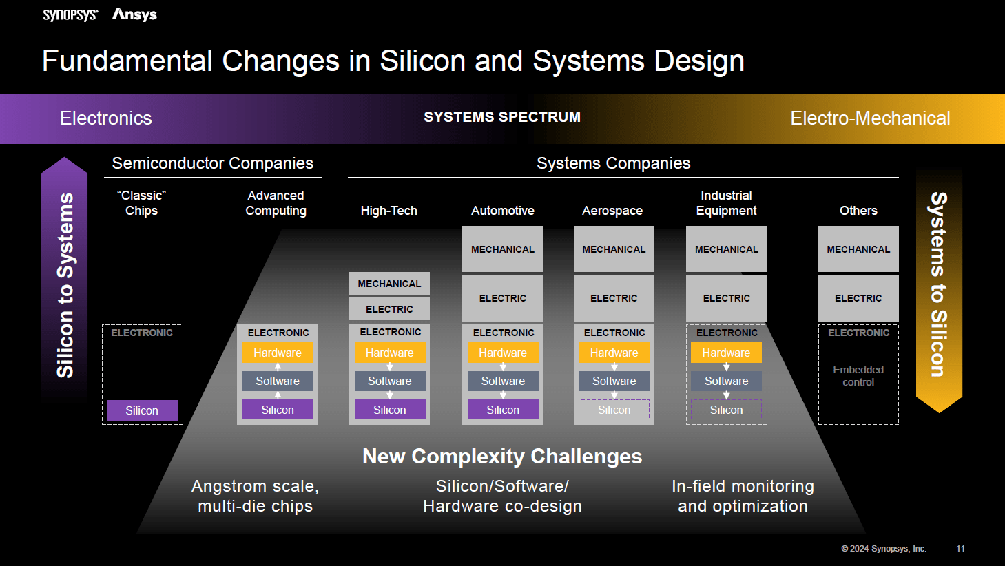
The rumors have been confirmed: after a seven-year partnership, on January 16th Synopsys and Ansys announced that they have entered into a definitive agreement under which Synopsys will acquire Ansys for an enterprise value of approximately $35 billion. The transaction is anticipated to close in the first half of 2025. Summing up Synopsys’ 2023 revenue (approximately $6 billion) and Ansys’ 2023 revenue guidance (approximately $2 billion), the combined entity is expected to achieve a $8 billion annual income. According to the two companies, this merger is motivated by a compelling rationale: first of all, the new customer demands stemming from the complexity of today’s intelligent systems (including the chiplet trend), which require the integration of semiconductor design and simulation and analysis, in a “silicon to systems” approach that fuses electronics and physics; besides that, new growth opportunities in areas such as automotive, aerospace and industrial, where Ansys has an established presence; and the complementarity of the two companies’ respective solutions. A key role in the integration of the two organizations will be played by Rick Mahoney, currently Chief Revenue Officer in the Go-to-Market Group at Synopsys and previously Senior Vice President of Worldwide Sales, Customer Excellence, and Marketing at Ansys.
As the company announced with a post on X (Twitter), “Intel Oregon welcomes major components of ASML first shipped High-NA EUV technology to help enable the continued and relentless pursuit of Moore’s Law.” Is this new piece of equipment going to help Intel advance its “5 nodes in 4 years” program? According to SemiAnalysis, double patterning with the “traditional” EUV litho equipment (low numerical aperture) is still a better option – in terms of cost and throughput – than single patterning with the new high numerical aperture litho equipment.
Credit: Intel
Let’s now move to more news, catching up on some of the updates from the last thirty days or so.
Synopsys to reportedly buy Ansys
It looks like the EDA oligopoly is bound to always be restricted to just three big companies. According to a January 5 report from The Wall Street Journal, Synopsys is in advanced talks to acquire Ansys for around $35 billion in a stock-and-cash deal. Reportedly, the two companies are now in exclusive negotiations. Rumors started with a December 22 Reuters exclusive report revealing that Synopsys had submitted an offer to acquire multiphysics simulation specialist Ansys. While the acquisition of Ansys would be a transformative event for Synopsys, there’s no doubt that the company co-founded by Aart de Geus has a long track record of acquiring other EDA players: just take a look at this list.
Let’s finish the year with a quick recap of some of 2023 events and trends.
New fab announcements
Geopolitical tensions continued throughout the year, prompting governments around the world to pass new subsidies – after the ones approved in 2022 – to support their respective semiconductor industries. Among them, the European Commission launched an €8.1 billion “Important Project of Common European Interest” on microelectronics; Japan is expected to invest $13 billion on semiconductors; and South Korea passed a “K Chips Act” tax credit plan.
The subsidies launched in 2022 – such as the US Chips Act and its European counterpart – spurred several new fab announcements in 2023: a partial list includes a Wolfspeed wafer fab in Saarland, Germany; a Texas Instruments wafer fab in Lehi, Utah; the expansion of an existing Microchip facility in Colorado Springs; a new capital injection to TSMC Arizona; an Infineon plant for analog/mixed-signal technologies and power semiconductors in Dresden, Germany; the choice of Chitose, Japan, as the site for the first Rapidus fab; the expansion of Applied Materials’ campus in Silicon Valley to build the “Equipment and Process Innovation and Commercialization” Center; the expansion of Analog Devices’ European headquarters in Limerick, Ireland, to build a new R&D and manufacturing facility; a joint STMicroelectronics-GlobalFoundries fab in Crolles, France; Intel factories in Kiryat Gat, Israel, and in Wrocław, Poland; Broadcom investments in Spain to build back-end semiconductors facilities; a CEA-Leti FD-SOI fab in Grenoble; the expansion of Analog Devices’ wafer fab in Beaverton, Oregon; a Silicon Box packaging facility in Singapore; the expansion of Infineon’s Kulim, Malaysia, SiC fab; a joint investment from TSMC, Bosch, Infineon and NXP on “European Semiconductor Manufacturing Company”, to be based in Dresden, Germany; an Amkor packaging and test facility in Peoria, Arizona. This is a list of announcements; real fabs will obviously take years to complete.


 Animation, 3D Art and 3D Models")