EDACafe Editorial Roberto Frazzoli
Roberto Frazzoli is a contributing editor to EDACafe. His interests as a technology journalist focus on the semiconductor ecosystem in all its aspects. Roberto started covering electronics in 1987. His weekly contribution to EDACafe started in early 2019. Nvidia’s computational lithography software; Arm to reportedly raise prices; hardware Trojans; downscaling spintronicsMarch 23rd, 2023 by Roberto Frazzoli
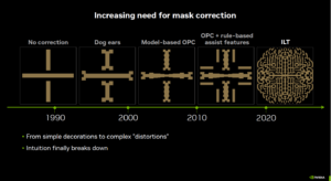
Manufacturing-related innovations make up a large part of this week’s news roundup. Arm vs Risc-V is also a theme, with the open-source ISA gaining ground in China while Arm’s IP is reportedly set to become more expensive. Nvidia cuts processing time for computational lithography The new Nvidia cuLitho software library for computational lithography promises to slash the time and energy required to produce photomasks. Mask manufacturing at advanced nodes requires a vey complex compensation of the pattern distortions caused by the diffraction of light or EUV rays. Simplistically explained, the compensation is essentially obtained by transforming the design polygons into complex shapes, so that the combined effect of these shapes and diffraction will eventually result in the desired polygons being projected on the resist. This transformation – an example of computational lithography – is obviously carried out by software running on a processing platform. With large chips now containing several dozen billion transistors, foundries working on advanced nodes need large datacenters to perform computational lithography. As we learn from Jensen Huang’s keynote given at this year’s GTC event, TSMC is currently using a 40,000 CPU server farm for computational lithography, absorbing 35 megawatts. With cuLitho, and running all parts of the computational lithography process in parallel, the workload can be handled by just five hundred Nvidia DGX H100 GPU-based systems, reducing power to ‘just’ 5 megawatts. According to Nvidia, in the near term, fabs using cuLitho could produce each day 3-5x more photomasks using 9x less power than current configurations. A photomask that required two weeks can now be processed overnight.
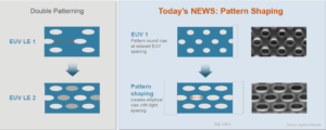
Arm to reportedly raise prices Arm is reportedly seeking to raise prices for its processor IP, as it aims to boost revenue ahead of an initial public offering in New York. The British firm recently notified several of its customers of a “significant shift” to its business model. Arm reportedly intends to alter its royalty program, ceasing to charge chipmakers royalties for using its IP based on a chip’s value, and instead charge device makers based on the much higher value of the end product – e.g. a smartphone. MediaTek, Unisoc, Qualcomm, Xiaomi and Oppo are among the companies that have been made aware of the proposed changes to pricing policy, the report added. Baidu invests on StarFive Shanghai-based Risc-V vendor StarFive has reportedly received a strategic investment ($146.46 million) from Chinese search giant Baidu. According to Reuters, StarFive was established in 2018 as a “China-facing offshoot” of California-based SiFive. The Baidu investment reflects a growing trend among Chinese tech giants. Earlier this month Alibaba’s chip unit T-Head and payment service Alipay jointly announced they will develop chips for secure payments based on Risc-V. Avoiding EUV double patterning Applied Materials’ new Centura Sculpta patterning system offers chipmakers an alternative to EUV double patterning when it comes to obtain certain specific features beyond the spacing resolution limit of EUV. In the example provided by the company, double EUV patterning is used to reduce tip-to tip spacing between elliptic interconnect vias: the first patterning only includes ‘every other’ via, then the second patterning adds the vias in between. With Centura Sculpta, instead, one single EUV patterning is used to create round vias, one for each of the elliptic vias that need to be created; this does not violate the spacing resolution limit of EUV, since round vias are smaller than the final elliptic vias. Then all round vias are widened in the same direction, by means of an oblique “ribbon beam” that hits the vertical sidewalls inside holes and removes the materials stack. By removing excess material, all round vias are “stretched” in the right direction and become elliptic vias. The process is described in this video. According to Applied Materials, avoiding double EUV patterning (and its associated added manufacturing process steps) can provide chipmakers with capital cost savings of approximately $250 million per 100K wafer starts per month of production capacity; manufacturing cost savings of approximately $50 per wafer; energy savings of more than 15 kwh per wafer; direct greenhouse gas emissions reduction of more than 0.35 kg of CO2 equivalent per wafer; and water savings of approximately 15 liters per wafer. The solutions can also potentially improve yield, as double patterning requires extreme – and difficult to achieve – precision in the overlapping of the two EUV exposures. Detecting hardware Trojans A group of researchers from German and Belgian academic and research institutions has presented what they believe is the first work in the public literature to perform and document a comprehensive hardware Trojan detection case study on full ICs over multiple CMOS technology generations (90 nm, 65 nm, 40 nm and 28 nm). The expression “hardware Trojans” refers to malicious design modifications that could take place during the outsourced manufacturing process, for example in the foundry. Despite the fact that the fundamental techniques to detect hardware Trojans that require evident changes to the silicon layout (e. g., adding or replacing logic cells) are nowadays well-understood, there exist only few public case studies describing and documenting the process in its entirety. Trojans are found by detecting all differences between digital layout and manufactured device by means of a GDSII–vs–SEM-image comparison. Scaling spintronic devices below 5-nanometer on standard CMOS Researchers from the University of Minnesota and the National Institute of Standards and Technology (NIST) have shown that iron palladium can be scaled down to much smaller sizes than the standard spintronic material, cobalt iron boron, and that it grow on top of a semiconductor industry-compatible CMOS substrate. . The research work paves the way to scaling spintronic devices down to smaller than five nanometers. Growing iron palladium was achieved on an 8-inch wafer-capable multi-chamber ultrahigh vacuum sputtering system. Acquisitions Renesas will acquire Austria-based Panthronics in an all-cash transaction. Panthronics specializes in Near-Field Communication (NFC) applications in fintech, IoT, asset tracking, wireless charging, and automotive. |
|
|
|||||
|
|
|||||
|
|||||


