


EDACafe Editorial Roberto Frazzoli
Roberto Frazzoli is a contributing editor to EDACafe. His interests as a technology journalist focus on the semiconductor ecosystem in all its aspects. Roberto started covering electronics in 1987. His weekly contribution to EDACafe started in early 2019. Special report: 2023 SEMI Industry Strategy Symposium EuropeFebruary 23rd, 2023 by Roberto Frazzoli
European company executives and analysts got together to discuss old continent’s strengths and weaknesses, aiming to make the most of the subsidies that the EU Chips Act will provide to the European semiconductor ecosystem Necessary but not sufficient: this is how the EU Chips Act – the subsidy plan recently passed by the European Union to support Europe’s semiconductor industry – is perceived by many of the company executives and analysts convened in Vienna on February 15th and 16th for the 2023 edition of the annual SEMI European Industry Strategy Symposium. Organized by SEMI Europe – regional office of the global industry association representing the electronics manufacturing and design supply chain, the event attracted over two hundred attendees and offered valuable insights on a number of themes that are expected to impact not just the old continent, but also its geopolitical and technological partners in America and Asia. The two-day symposium saw the participation of over thirty speakers and offered three panel discussions. 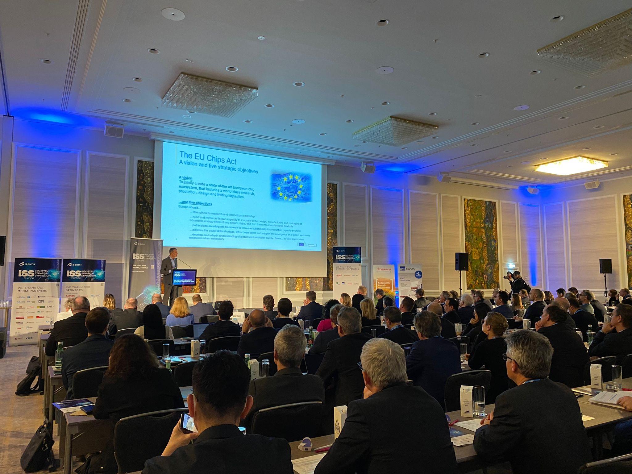 Credit: SEMI Europe In this article we will briefly summarize some of the symposium content – starting with the welcome remarks from Laith Altimime, President of SEMI Europe. Altimine outlined SEMI Europe’s agenda to make the European Chips Act a success: focus across the whole manufacturing ecosystem (materials, chemicals, gases, design, equipment, manufacturing and RTOs) to support supply chain resilience and industry growth; pursue stakeholders’ collaboration to achieve industry sustainability goals, considering that the industry has the urgent need of introducing smart and green manufacturing solutions and pave the way to net zero; support Europe’s talent pipeline transformation with concrete funds and investments, to close the talent gap and cultivate the workforce of tomorrow; foster industry participation – through the European Semiconductor Board – to ensure expertise-based decision making and inclusive governance; leverage the European “chip diplomacy”, going forward as one on export control, investments, supply chain as well as innovation and R&D.
Updates on the EU Chips Act Let’s go straight to an update on the implementation roadmap of the EU Chips Act, which was provided by a representative of the European Commission (the executive of the European Union), Francisco Ibáñez from the DG Connect (Directorate-General for Communications Networks, Content and Technology). The next steps will be crucial: start of the negotiation between co-legislators is scheduled for March 2023; the official adoption of the Chips Act is expected for the end of Q2 2023, followed by the finalization of proposal for the Chips Joint Undertaking (JU); and the entry into force of both Chips Act and Chips JU is scheduled for Q3 2023. Ibáñez also provided details on one of the pillars of the EU Chips Act, the “Chips for Europe Initiative”. Key to this part of the program will be the creation of a design platform to reduce entry barriers and administrative burden for EU companies engaging in chip design; and the establishment of a set of new pilot lines for technologies such as scaled FD-SOI down to 10-nanometers and below, leading-edge process technology at 2-nanometers and below, and advanced heterogeneous system integration. Is the EU Chips Act sufficient to cope with de-globalization? An analysis squarely challenging some of the most optimistic expectations raised by the EU Chips Act was provided by Michael Alexander, partner of consultancy firm Roland Berger’s Advanced Technology Center. Alexander examined the EU subsidy plan in the context of the de-globalization currently faced by the semiconductor industry. Aspects of de-globalization include China’s plan to boost domestic chip production with the goal of covering 70% of its own IC market by 2025; China challenging Taiwan’s integration into the Western ecosystem; US sanctions imposed on China to disrupt advanced semiconductor supply chains; and prominent companies (Apple, Samsung, Microsoft, Google, carmakers) starting to renew their supply chain to gain independence from China. According to the analyst, de-globalization fosters commercially unfavorable approaches, and is driving the industry into what can be described as a “war for technology”. This adds to a preexisting situation that has seen Europe’s position in the semiconductor industry constantly deteriorating over the past decade: from 2013 to 2022, the European share of semiconductor capacity fell from 13.7% to 7.4% for 12” wafers, and from 16.4% to 14.1% for 8” wafers. According to Alexander, compared to other countries’ similar initiatives, the European Chips Act seems to be too small, too slow and too unfocused. As for focus, the analyst reminded that – despite the presence of world leading OEMs such as European carmakers – Europe’s semiconductor market shares in automotive and industrial applications are relatively small: 37% and 17% respectively. Similar figures were provided by Ibáñez. The EU Chips Act should therefore prioritize the process technologies that are most relevant to automotive and industrial applications, which include mature nodes. 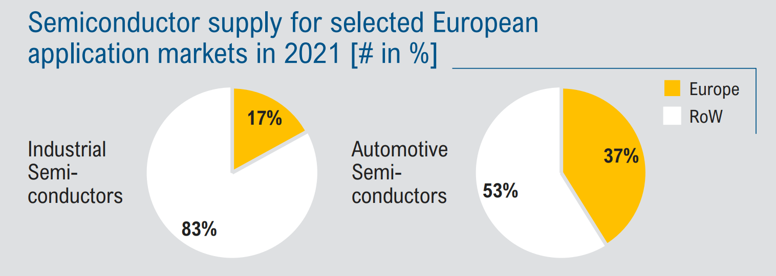 Source: Roland Berger presentation Taking stock of the situation: 2023 market forecasts, with a -22% downturn warning Before delving into topics more directly related to the long-term targets of the EU Chips Act, let’s take a look at the 2023 market forecasts provided by two analysts, sharply different from one another. Guillaume Girardin from France-headquartered Yole Intelligence said Yole expects a 2023 semiconductor total market decline of approximately -9%. Contributing to this trend are the trade war and tensions between US and China, a weak GDP growth, as well as a moderate global economic recession caused by inflation, hitting the consumer demand that supports 60% of the semiconductor industry. Demand lowest point should be reached by Q3 2023. Veteran market analyst Malcom Penn, however, is forecasting a -22% decline for 2023. According to the CEO of British market research firm Future Horizons, every single warning light is currently flashing red, including the increase in production capacity (new fabs) coincident with softening market demand, and the uncertain economy outlook with high inflation and interest rates. Penn also claimed he was able to predict the 2021 boom and the 2022 shortage, since the semiconductor industry continues to be predictable as it is still based on market boom-bust cycles. The seventeenth industry down cycle is now in full flow. “Prepare for the double-digit recession, there are no soft landing,” he said. However, “the seventeenth industry upturn is just around the corner.” On a longer term, though, everybody expects a strong semiconductor market growth driven by AI, automotive etc. Michael Anfang, Executive Vice President of STMicroelectronics for Sales & Marketing, EMEA, offered some examples of the growth of semiconductor content in end products. In cars, the Electronic Stability Control function used to employ just three ICs in 2018 and equipped just 30% of models, whereas next generation ESC will need thirteen ICs and will be adopted by 70% of vehicles. In robot lawnmowers, the number of 32-bit microcontrollers climbed from four in 2013 to twelve in 2019. Europe’s strengths Getting back to the EU Chips Act, the symposium offered a sort of ‘inventory’ of some of Europe’s existing strengths that can serve as a foundation for further developments fostered by the upcoming subsidies. Assets include a leadership position in some specific semiconductor processes: this is the case of Silicon-on-Insulator, a key part of the offering of France-based Soitec. Pierre Barnabé, Chief Executive Officer & Director of the company, said that Soitec’s technology is inside every 4G and 5G smartphone, as all smartphone makers are using RF front-end modules based on Soitec’s RF-SOI substrates. Incidentally, the European SEMI Special Service Award was presented to FD-SOI pioneer Thomas Skotnicki (Warsaw University of Technology, Poland) during the symposium. More European assets concern some key equipment technology, besides the universally known EUV lithography tools built by ASML; and, in addition to that, Europe research institution are actively pursuing R&D initiatives on emerging technologies. Below we will provide a quick overview of this scenario. Multi-beam mask writing Starting from the early steps of the manufacturing flow, one of the leading players in the area of advanced mask writing – namely, the masks used in EUV lithography – is Austria-based IMS Nanofabrication. Diffraction at smaller nodes requires ‘inverse lithography technology’, which could simplistically be described as a pre-distortion of the mask pattern to compensate for the opposite distortion in the projection phase. For example, to avoid corner rounding on the projected pattern, corners must be protruding in the mask pattern. Writing these complex shapes takes a very long time – up to sixty hours or more – with conventional single-shot mask-writing equipment, such as Variable Shaped Beam Writers; to solve this problem, in 2016 IMS came up with its multi-beam mask writing technology. The solution is based on an aperture plate system that splits an electron beam into over 260,000 beamlets that can be individually deflected, enabling pixel-based writing. This way, mask writing time can be reduced to less than twelve hours. As explained by Mathias Tomandl, Head of Customer Accounts & Projects Operations Division at IMS, the company is now developing new equipment to extend its multi-beam technology to mature nodes. 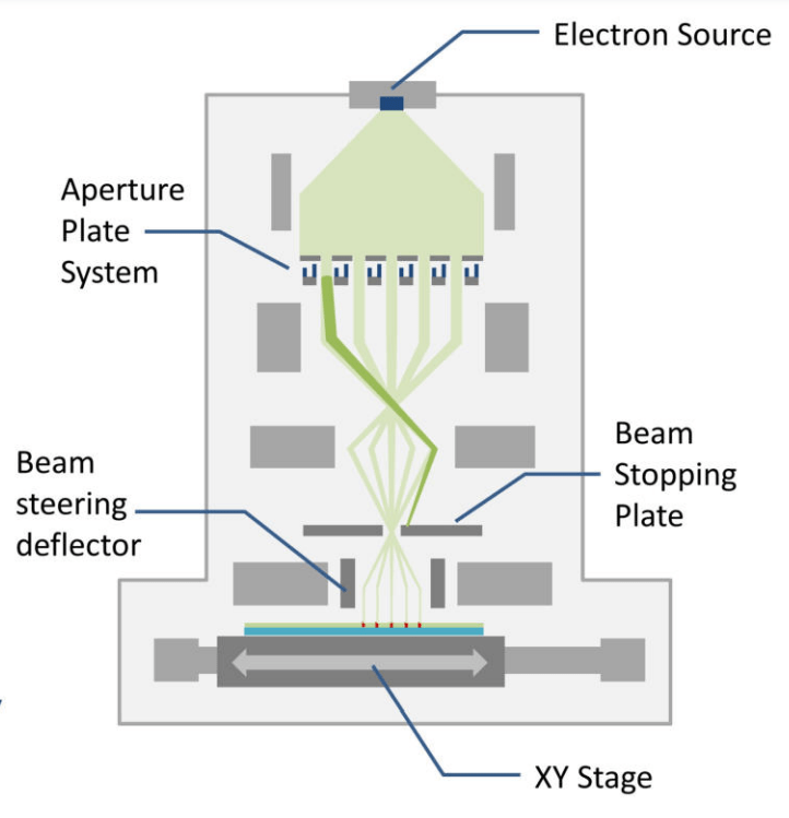 Structure of a multi-beam mask writer. Copyright: IMS Nanofabrication X-ray inspection of advanced packaging Moving to the other end of the manufacturing flow, Dionys van de Ven, President of Germany-based Comet Yxlon, explained the benefits of the company’s X-ray equipment for the inspection of advanced packaging characterized by complex 3D architectures – which make it possible to obtain high-resolution insights of C4 bumps in less than five minutes. Packaging inspection is needed in process development, process monitoring and excursion control, to reduce time-to-market and increase yield. EU R&D initiatives in AI and quantum computing European assets that the EU Chips Act could leverage include world-class research and development institutions and programs, some of them now engaged in emerging technologies such as AI or quantum computing. Steven Latré, Fellow AI at imec, described the Belgian research institute’s artificial intelligence roadmap and achievements. Latré pointed out that the size of neural networks is growing at a factor 100 per year, therefore new solutions are needed to avoid hitting a power wall. To reduce AI power consumption, imec is betting on spiking neural networks (with four different chips, the biggest one encompassing over one million neurons) and on software-hardware co-optimization.  Source: Steven Latré (imec) presentation Mika Prunnila from the VTT Technical Research Centre of Finland described a EU-funded program aiming at the construction of a quantum technology pilot line. Called Qu-Pilot, the initiative is funded by a 19 million euro grant and involves twenty-one European partners – among them imec, Fraunhofer, CEA-Leti – coordinated by VTT. The program will also develop improved test facilities for the test and qualification of quantum devices. Sustainability: semiconductors as part of the problem and the solution A large part of the symposium was devoted to the sustainability theme – which SEMI has recently addressed also with a white paper. In fact, this topic is tightly related to the above-described asset scenario, since some of the sustainability solutions being proposed also represent additional European strengths. The SEMI event addressed both aspects of the relationship of the semiconductor ecosystem with the sustainability theme: on the one hand, semiconductors are part of the problem – since fabs use energy, water, and toxic substances – but on the other hand they are also part of the solution with the efficiency advancements enabled by wide-bandgap materials and other power reduction efforts. Measuring the environmental impact of semiconductor fabrication Marie Garcia Bardon, R&D Manager at Belgian research institute imec, described the Sustainable semiconductor technologies and systems (SSTS) program aimed at reducing the carbon footprint of the semiconductor industry. The speaker reminded that emissions grow at every new process node, and this – combined with other market and technology trends – will lead to a dramatic increase of carbon footprint if no countermeasures are taken. “Doing nothing is not an option,” she said. Instruments being developed within the SSTS program include the imec.netzero online tool, which will enable chipmakers to ‘shift left’ the sustainability calculations for new designs, moving from just PPA to PPACE metrics , where C stands for Cost and E for Environmental Cost.  The imec.netzero online tool will be publicly available in June. Copyright: imec Recycling process gases Moving to chip fabrication, UK-headquartered Edwards is developing solutions to reduce the carbon footprint of semiconductors fabs. As explained by Chris Bailey, VP of emerging technologies, the company is testing – in collaboration with imec – a system for hydrogen recovery and recycling from EUV lithography equipment. With an expected recovery rate of 83%, the solution will provide a 54% reduction in total energy input (including H2 production energy) and equivalent CO2 savings of 97 tonne per year per EUV tool. The company is also developing a system for noble gas recovery and recycling from etch process steps, mainly targeted at krypton or xenon. The system is expected to significantly reduce the eCO2 impact of etch as these gases have a very high ‘embodied energy’ – that is, it takes a lot of energy to produce them by separation from air. Additionally, Edwards is developing a system for reducing NOx emissions from CVD process steps, which has achieved up to 50% reduction in NOx emissions when treating gases such as N2O. Reducing energy consumption with hybrid bonding Proceeding to advanced packaging solution – increasingly important with chiplet-based devices gaining traction – Chris Scanlan, SVP Technology at Netherlands-headquartered Besi, spoke about the benefits of hybrid bonding in energy efficient 3D chiplet designs. Hybrid bonding creates an ultra-fine pitch 3D connection directly between copper interconnects of the substrate wafer and the device die. This technology is already being used by AMD, by Intel for its Quasi-Monolithic Chip (QMC) architecture, and by TSMC for its SoIC solution – providing benefits in terms of density, latency and energy per bit. Besi is also taking measures to reduce the power consumption of its hybrid bonders. 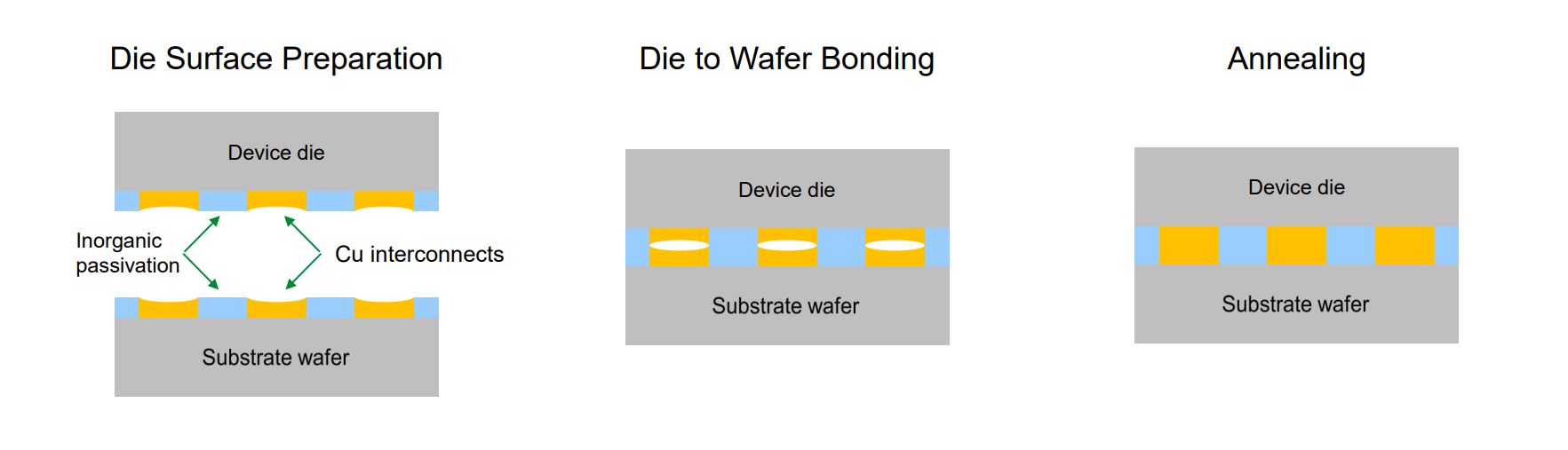 Steps of hybrid bonding. Copyright: Besi For a holistic approach to carbon footprint reduction, Schneider Electric – a founding member of the Semiconductor Climate Consortium – offers semiconductor companies its ‘supply chain decarbonization’ programs, as explained by Dallal Slimani, VP of the company’s Semiconductor Segment. Europe’s position in wide-bandgap materials Getting to the other side of the coin – semiconductors enabling sustainable solutions – Sabine Herlitschka, Chief Executive Officer of Infineon Austria, reminded that from 2010 to 2022 the energy consumption of data centers has remained the same despite a twelve-fold increase of Internet traffic and a 60% increase of data center workload. Today, key to the improvement in energy efficiency are wide-bandgap materials such as silicon carbide and gallium nitride. Herlitschka observed that GaN on silicon has intrinsic defect density and is therefore much more challenging than production-proven silicon. Addressing these challenges, Infineon Austria coordinated three EU-funded research programs on GaN. “The EU Chips Act needs to strengthen the competitiveness of Europe. I would not be satisfied by resilience only,” Herlitschka concluded. Infineon has recently announced investments in new capacity for wide-bandgap power components in its fabs in Villach, Austria, and Kulim, Malaysia. 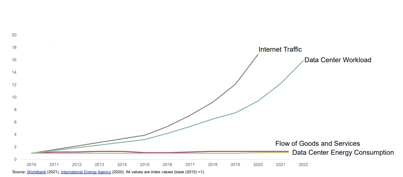 Source: Infineon Austria presentation Above-mentioned Soitec is also engaged in wide-bandgap materials: according to CEO Pierre Barnabé, the company’s Smart SiC technology enables a 20% increase in electric vehicles’ mileage. Challenges to support the European startup ecosystem Besides leveraging Europe’s strengths, the EU Chips Act is also expected to address old continent’s weaknesses such as the difficulties faced by startups or the semiconductor talent shortage. As for the first theme, Malcolm Penn jokingly said that in Europe if you tell your girlfriend that you work for a startup, she will leave you. Rebecca Dobson, Corporate Vice President EMEA at Cadence, addressed the startup topic by listing a series of Europe-specific challenges: seed and A round funds are often small; startups are often slow in scaling; lack of interest from major investors; and lack of a rigorous legislation preventing successful startups to be acquired by non-EU companies. Dobson said that Cadence is working with many European startups, and proposed autonomous driving as an area in which Europe should aspire to leadership. An unsexy industry struggling to attract talent Moving to the talent shortage plaguing the semiconductor industry, it looks like convincing talented students – males and females – to choose a STEM education path is not enough, as other tech-based sectors are much more attractive to them. “The semiconductor industry is not perceived to be sexy. The hyperscalers are,” observed Cadence’s Rebecca Dobson. Clara Haubenwallner, Student Assistant at Graz University of Technology (Austria), suggested that to attract young talent the semiconductor industry should stop advertising itself with pictures of people wearing bunny suits and holding wafers. Several speakers recommended to let the world know how important semiconductors are in improving our life and protecting the environment. To this goal, Malcom Penn jokingly suggested to put a “silicon inside” sticker on coveted end products. Monitoring the industry’s skill needs Skill shortage in the European semiconductor industry is being monitored by the METIS initiative (MicroElectronics Training Industry and Skills), co-funded by EU resources. Léo Saint-Martin, Associate Consultant of the consulting firm that manages the initiative, summarized the results from the latest monitoring. Among other findings, the survey showed a very severe shortage for specific senior profiles such as advanced systems architecture designers, highly skilled analog designers, and experts in specific applications fields. New factors influencing the job market include the rise of investments in manufacturing capacities (leading to higher recruitment needs and to a focus on production process engineers, maintenance technicians, etc.) and the semiconductor shortage (requiring skills to handle supply-chain management and logistics). Talent shortage translates into the necessity to hire foreign candidates, therefore METIS recommends favoring intra and extra-EU mobility. To support the industry, METIS is planning to build an online platform regrouping microelectronics courses and an EU Chips Skills Alliance. Conclusion “The time has come,” said Leonard Hobbs, General Manager of ‘MIDAS Ireland’ electronics cluster, expressing his optimism for the chances of success of the EU Chips Act. “This time it’s different,” he added, referring to previous EU-funded initiatives aimed at bolstering the European semiconductor industry. A less optimistic tone was used by Michael Alexander, Partner of Roland Berger, urging companies to take action: “This is the last call,” he said. “We need to be more paranoid about semiconductors, even in Europe,” he added, quoting Andy Grove. “We cannot wait for others to take action.” It’s probably too early to strike the right balance between optimism and worries, as some pieces of the puzzle are still missing. Will an injection of taxpayers’ money help overcome longtime structural and cultural obstacles such as the conservative approach of European venture capital towards startups? Will European OEMs, carmakers in the first place, provide a strategic support to the efforts of their European chip suppliers? Will any of the European carmakers become a vertically integrated player such as Tesla, developing its own chips? More uncertainty factors are linked to the current global geopolitical shakeup, which seems to be far from over – with war in Ukraine, tensions on Taiwan, and multiple Chips Acts around the world. Assuming that the outcome of this shakeup will be a new world order in which one of the major geopolitical blocs will encompass the US, the European Union, and some Asian partner countries, reinforcing the coordination of semiconductor strategies at the bloc level could probably facilitate bloc-level independence and resilience – while saving individual countries the effort to fill their respective semiconductor ecosystem gaps. |
|
|
|||||
|
|
|||||
|
|||||


 Animation, 3D Art and 3D Models")