Open side-bar Menu
 EDACafe Editorial

Archive for March, 2022

Nvidia’s innovations; secure design; cloud-based EDA; Risc-V tools; early-stage investments

Friday, March 25th, 2022

Both Nvidia and Arm are in the news this week, obviously for unrelated reasons after the proposed acquisition deal collapsed. Nvidia keeps introducing impressive innovations at an impressive pace, raising the bar for contenders. Meanwhile, Arm keeps preparing for its IPO – expected to value the company at $60 billion – with SoftBank reportedly planning to pick Goldman Sachs as the lead underwriter.

Nvidia GTC updates

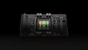
At its recent GTC event, Nvidia introduced a host of new products and innovations mostly targeted at AI-powered data centers; here we will only provide an extremely brief overview. As for GPUs, the company launched its new Hopper architecture, claiming an order of magnitude performance leap over its predecessor Ampere architecture. Nvidia also announced the first Hopper-based GPU, the H100, an 80 billion transistors chip built using a TSMC 4N process, offering nearly 5 terabytes per second of external connectivity and 3 terabytes per second of memory bandwidth. Among the innovations introduced by the H100 is a new Transformer Engine (devoted to the Transformer model for natural language processing); the second generation of the Secure Multi-Instance GPU technology; the fourth generation of NVLink; new DPX instructions to accelerate dynamic programming. A 71-page white paper on the H100 architecture can be downloaded from this web page. As for data center CPUs, Nvidia announced its first Arm Neoverse-based processor, called ‘Grace CPU Superchip’, comprising two CPU chips coherently connected over NVLink-C2C, a new high-speed, low-latency, chip-to-chip interconnect. The device integrates 144 Arm cores, reaching an estimated performance of 740 on the SPECrate 2017_int_base benchmark. Another announcement from the GTC event concerns NVLink-C2C, a chip-to-chip and die-to-die interconnect, open to custom silicon integration. NVLink-C2C enables coherent interconnect bandwidth of 900 gigabytes per second or higher. In addition to it, Nvidia will also support the Universal Chiplet Interconnect Express (UCIe) standard announced earlier this month. Recent updates also include Nvidia reportedly interested in exploring chip manufacturing with Intel Foundry Services.

Nvidia H100. Credit: Nvidia

(more…)

Intel to invest in Europe; Arm to reportedly cut workforce; SiFive gets more funding; research updates

Thursday, March 17th, 2022

Despite SEMI’s reassuring statement, concerns of a potential neon gas shortage due to the Ukrainian war keep surfacing. According to sources contacted by Reuters, effects on chip manufacturing could be felt if the conflicts drags on, and could mostly hit smaller chipmakers. On a wider IT scale, recent updates include concerns about data security expressed by some European governments in countries – Germany and Italy – that rely on Russia-headquartered Kaspersky’s cyber protection technologies. Moving to EDA companies, Aldec has suspended all sales and distribution transactions in Russia and is offering temporary housing to its Ukrainian personnel at a company’s facility in Poland; and Ansys, that had already suspended all sales transactions and consulting activities in Russia and Belarus, has now announced it will also make a financial contribution to ‘Doctors Without Borders’ in support of Ukrainian refugees. Let’s now move to tech news, this week including some academic research updates.

Intel investments in Europe

The European Union’s initiative to bolster local chip manufacturing (“EU Chip Act”) is starting to bear fruits: Intel has just announced the first phase of its plans to invest 80 billion euros in the European Union over the next decade along the entire semiconductor value chain. The plan includes a 17 billion euros investment for two semiconductor fabs in Magdeburg, Germany, a site that Intel has dubbed ‘Silicon Junction’. More Intel investments are planned in Ireland, Italy, Poland, Spain and France. In this latter country Intel is planning to establish its new European R&D hub, its European headquarters for high performance computing and artificial intelligence design capabilities, and its main European foundry design center.

(more…)

Wafer-on-Wafer; ExaFlops supercomputers; Arm management change; Canadian battery plants

Thursday, March 10th, 2022

IDC is among the first market research firms trying to provide an initial assessment of how the Ukraine war will affect ICT spending and technology markets worldwide. Consequences are expected on many aspects of the business environment – and will arguably affect the semiconductor ecosystem, too. Hoping for peace, let’s now move to some tech news.

Incubators updates: Analog Devices (Ireland), Infineon (Hong Kong)

Analog Devices will invest €100 million over the next three years in ADI Catalyst, a 100,000 square foot custom-built facility for innovation and collaboration located at its campus in the Raheen Business Park in Limerick, Ireland. This latest phase of expansion will also see the creation of 250 new jobs in the Irish market by 2025. The Catalyst project is supported by the Irish Government through IDA Ireland.

Hong Kong Science and Technology Parks Corporation (HKSTP) has partnered with Infineon Hong Kong in a three-year co-incubation program targeted at microelectronics startups.

Advanced packaging and 3D updates: Apple’s Ultrafusion, Graphcore’s Wafer-on-Wafer

Apple has recently announced M1 Ultra, its new Arm-based SoC that will power the next Mac personal computers. The device uses Apple’s UltraFusion packaging architecture to interconnect the die of two M1 Max chips through a silicon interposer conveying more than 10,000 signals, providing 2.5TB/s of low latency bandwidth. This enables M1 Ultra to behave and be recognized by software as one chip, so developers don’t need to rewrite code. The new SoC consists of 114 billion transistors and features a 20-core CPU, a 64-core GPU, and a 32-core neural engine.

Graphcore has recently unveiled what it claims is the world’s first 3D Wafer-on-Wafer processor – the Bow IPU – built using TSMC’s Wafer-on-Wafer 3D technology. In the new device, two wafers are bonded together to generate a new 3D die: one wafer for AI processing, which is architecturally compatible with the preexisting Graphcore GC200 IPU processor, and a second wafer for power delivery die. By adding deep trench capacitors in the latter die, right next to the processing cores and memory, Graphcore claims to be able to deliver power much more efficiently – enabling a 40% increase in performance. More details have been disclosed in this EETimes article. As the company explained, the two wafers are bonded – metal sides together – without any interstitial bumps, in a sort of cold weld, achieving an extremely high density of interconnect. The device also uses ‘back-side through-silicon vias’ (BTSVs) which allow connection to layers inside the wafer sandwich. Graphcore points out that Wafer-on-Wafer is different from chip-on-wafer technologies, and that aligning two entire wafers is easier rather than two die. This – along with the use of an ion etch process for BTSVs – results in a finer connection pitch.

Graphcore has also announced it will use the next generation of its IPU technology to build an AI supercomputer that will reach over 10 ExaFlops of AI floating point compute. The system – called ‘the Good Computer’ in honor of computer science pioneer Jack Good – is expected to be available by 2024.

(more…)

Intel’s German fab; chiplet interconnect standard; Qualcomm’s 3nm foundry order; Altair acquires Powersim; impact of Ukraine war

Thursday, March 3rd, 2022

The unrelated themes of war in Ukraine and semiconductor investments crossed each other on TV screens last Tuesday when Intel’s CEO Pat Gelsinger appeared with a Ukrainian flag on his jacket during the State of the Union Address. Gelsinger, whom President Joe Biden gave a shoutout praising Intel’s plan for a mega-fab in Ohio, attended the speech as a guest in the First Lady’s viewing box. Ukraine war is also a topic of our news roundup this week, as we try to monitor its impact on the semiconductor ecosystem and on IT in general. But first, some industry updates.

EDA updates: Breker, Mirabilis, open source FPGA tools

Breker Verification Systems has unveiled SystemUVM, a framework designed to simplify specification model composition for test content synthesis with a UVM/SystemVerilog syntactic and semantic approach familiar to universal verification methodology (UVM) engineers. According to Breker, by leveraging synthesis for test content generation, a 5X improvement for larger components and multi-IP subsystems is common in composition time combined with significant coverage increases.

Mirabilis Design has released its new VisualSim MicroArchitecture Modeler, what it claims is the first solution to enable verification of the micro-architecture of the entire SoC at cycle-per-cycle. According to Mirabilis, processor core vendors do not provide cycle-accurate models for high-end cores. Instead of resorting to expensive emulators or extremely slow RTL execution, VisualSim MicroArchitecture Modeler runs 10000+ instructions per second and still maintain a 85-95% accuracy. The solution employs a library of customizable IP components.

(more…)


© 2025 Internet Business Systems, Inc.
670 Aberdeen Way, Milpitas, CA 95035
+1 (408) 882-6554 — Contact Us, or visit our other sites:
TechJobsCafe - Technical Jobs and Resumes EDACafe - Electronic Design Automation GISCafe - Geographical Information Services  MCADCafe - Mechanical Design and Engineering ShareCG - Share Computer Graphic (CG) Animation, 3D Art and 3D Models
  Privacy PolicyAdvertise