EDACafe Editorial Roberto Frazzoli
Roberto Frazzoli is a contributing editor to EDACafe. His interests as a technology journalist focus on the semiconductor ecosystem in all its aspects. Roberto started covering electronics in 1987. His weekly contribution to EDACafe started in early 2019. Moore’s Law extension a key theme at the 2021 VLSI SymposiaJune 5th, 2021 by Roberto Frazzoli
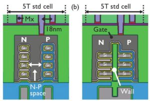
New materials, new transistor structures, new integration schemes: many of the boost scaling options being investigated by research teams around the world will be represented at the 2021 Symposia on VLSI Technology & Circuits – running as a virtual event from June 13 to 19. Just as a teaser, in this article we will briefly summarize a handful of papers from the Technology program, to give a taste of some current research trends. Benefits of forksheet over nanosheet One of the papers presented by Belgian research institute Imec is meant to demonstrate the benefits of forksheet transistors over nanosheet transistors for CMOS area scaling. Forksheet devices are lateral nanosheet devices with a forked gate structure. The physical separation of N- and PFETs by a dielectric wall enables N-P space scaling and consequently sheet width maximization – compared to a N-P nanosheet configuration – for the same footprint. According to Imec, forksheet transistors offer additional benefits in the manufacturing process. Firstly, for nanosheets the high mask aspect ratio is challenging for patterning a well-defined N-P boundary over the full stack height. Secondly, the pWFM (Work Function Metal) lateral etch in-between NMOS nanosheets can lead to mask undercut and therefore pWFM removal from PFETs. For forksheet devices, the mask aspect ratio at the N-P boundary is substantially lower because the mask edge lands on top of the wall. In addition, the risk of pWFM removal from PFETs due to mask undercut is eliminated by the physical separation of the pWFM on either side of the wall, including along the gate trench side walls. Electrostatic control for forksheets and nanosheets is comparable.
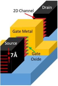
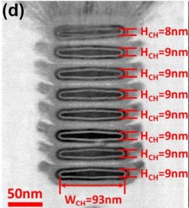
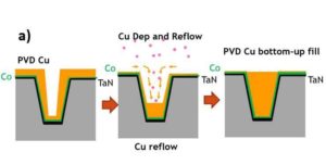
Transition metal dichalcogenides promise ultimate CMOS scaling A paper from Intel will focus on Transition metal dichalcogenides (TMD), a type of 2D van der Waals (vdW) material, as a solution for further CMOS downscaling. TMD naturally provide sub-1nm channels with intrinsically passivated surfaces and favorable bandgaps that allow for good-mobility channels with strong electrostatic control required for transistor gate length scaling down to 5nm. Intel will present a comprehensive look at both NMOS and PMOS 2D transistors fabricated with monolayer (ML) MBE and CVD grown films, both transferred and directly grown at a selected area. The paper will also present methods for vdW interface engineering through atomic layer deposition (ALD), thermal and evaporation processes. Gate-oxide interface engineering through metal seeding and ALD demonstrates that a single 2D channel material can selectively make PMOS or NMOS transistors, alike Si CMOS. Engineered interfaces, novel contact and area-selective seeded growth methods are demonstrated to advance the state of 2D vdW NMOS and PMOS transistors and to move toward manufacturable fabrication. Improving the performance of GAA transistors with channel stacking and Ge-Si National Taiwan University will present a paper on the benefits and manufacturability of gate-all-around (GAA) devices using channel stacking to further enhance the drive current for a given footprint. Additionally, the devices developed by the Taiwanese researchers employ Germanium-Silicon, as Ge is an attractive option for high mobility channel to boost the drive current, thanks to its intrinsic higher mobility as compared with Si. The work demonstrates an 8-stacked nanosheets and 7-stacked nanowires realized by H2O2 wet etching. Among the results achieved, a high inter-channel uniformity and a record ION, 110μA per stack (4100μA/μm per channel footprint). Simple wet etching can reach the sufficient selectivity to fabricate the highly uniform nanosheets and nanowires. Even higher number of stacked channels (>8) is expected to further enhance the ION. Extending the Dual Damascene BEOL to the nanosheet era A paper by IBM and Applied Materials will demonstrate the scalability of the dual damascene (DD) integration scheme for BEOL interconnects below 28 nm pitch. According to IBM, even though alternative processes have been proposed for the interconnect metallization and integration flow in the nanosheet era – such as subtractive patterning and single damascene – DD is still the most economical integration path thanks to its minimal processing steps and its maturity. The team developed and demonstrated two novel process flows. First, they extended Cu-based damascene interconnect with a selectively deposited TaN barrier that reduced via resistance without compromising reliability. Second, they introduced an innovative dual metallization scheme with metallurgy chosen for the enhanced performance of fine and wide lines. These process innovations enable a significant improvement in via, signal and power line resistances. The Cu/R-TaN/SB and Co/Cu composite metallization schemes combined with a higher modulus dielectric can overcome DD scaling challenges with better gap-fill, reduced via R (50%) and line R (20% for Co/Cu comp), and improved line roughness in 10-12nm width structures. The higher wide line R and corresponding IR gain for Co/Cu comp can be reduced through use of higher aspect ratio wide lines. The Co/Cu comp interconnects are the optimal solution for HPC-type design layouts, whereas for mobile like layouts the Cu/RTaN/SB provides easy path for Cu extension. Indium oxide transistors for BEOL-compatible 3D integration Purdue University (West Lafayette, IN) will present a work on transistors built with Indium oxide (In2O3), a promising material for back-end-of-line (BEOL) compatible transistors for monolithic 3D integration. In this work, the performance of atomic layer deposition In2O3 transistors is further enhanced by channel thickness engineering and post-deposition annealing. In summary, high-performance 3D Fin transistors and integrated circuits based on BEOL compatible oxide semiconductor by ALD are demonstrated by this work for the first time. High mobility of 113 cm2/V⋅s and record high maximum drain current of 2.5 mA/μm are achieved. The demonstration of 3D devices and integrated circuits suggest ALD oxide semiconductors and devices have their unique advantages over sputtering films and are promising toward BEOL-compatible monolithic 3D integration for 3D integrated circuits. Moving the power delivery network to the wafer backside Another paper by Imec addresses the concept of moving the power delivery network to the wafer’s backside, to alleviate routing congestion on its frontside and therefore enable further scaling. According to the Belgian research institute, the solution allows a reduction of the VDD or IR-drop caused by increased metal line resistance in BEOL especially when combined with buried power rails (BPR) technology. Researchers demonstrated a solution for achieving this result by extreme wafer thinning and W-filled nano-through-Si-vias. Among other results, researchers observed no BTI (bias temperature instability) degradation. 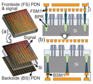 Moving power delivery networks from the frontside to the backside of wafers. Source: 2021 VLSI Symposia A rich event program The 2021 VLSI Symposia is actually two events in one – Technology and Circuits – and will therefore offer a rich program with hundreds of technical papers, workshops, short courses, panels and forums. Speakers scheduled to give plenary talks include Dr. Siyoung Choi, President, GM of Foundry Business, Device Solutions Division, Samsung Electronics; Dr. Om Nalamasu, SVP and CTO, Applied Materials, President, Applied Ventures; Prof. Satoshi Matsuoka, director at RIKEN Center for Computational Science; Mark Papermaster, chief technology officer and executive vice president of Technology and Engineering at Advanced Micro Devices. |
|
|
|||||
|
|
|||||
|
|||||


