


Catching up on some of the news from the last four weeks or so, the IBM 2-nanometer announcement definitely stands out as a major update. Several recent news also concerns EDA, as well as AI accelerators. Two of the newest updates about AI startups will translate into an additional $150 million pumped into this industry by investors.
IBM’s 2-nanometer chip
As widely reported by many media outlets, last May 6 IBM announced the development of the world’s first chip with 2-nanometer nanosheet technology. The result was achieved by IBM research lab located at the Albany Nanotech Complex in Albany, NY, where IBM scientists work in collaboration with public and private sector partners. According to the company, IBM’s new 2-nanometer chip technology will achieve 45 percent higher performance, or 75 percent lower energy use, than today’s most advanced 7-nanometer node chips. Reporting about the announcement, EETimes underlined that this chip is the first to use extreme-ultraviolet lithography (EUV) for front-end of line (FEOL) processes. Other details reported by EETimes include the use of bottom dielectric isolation to eliminates leakage current between nanosheets and the bulk wafer; and a novel multi-threshold-voltage scheme. Reportedly, IBM expects 2-nanometer foundry technology based on this work to go into production towards the end of 2024.
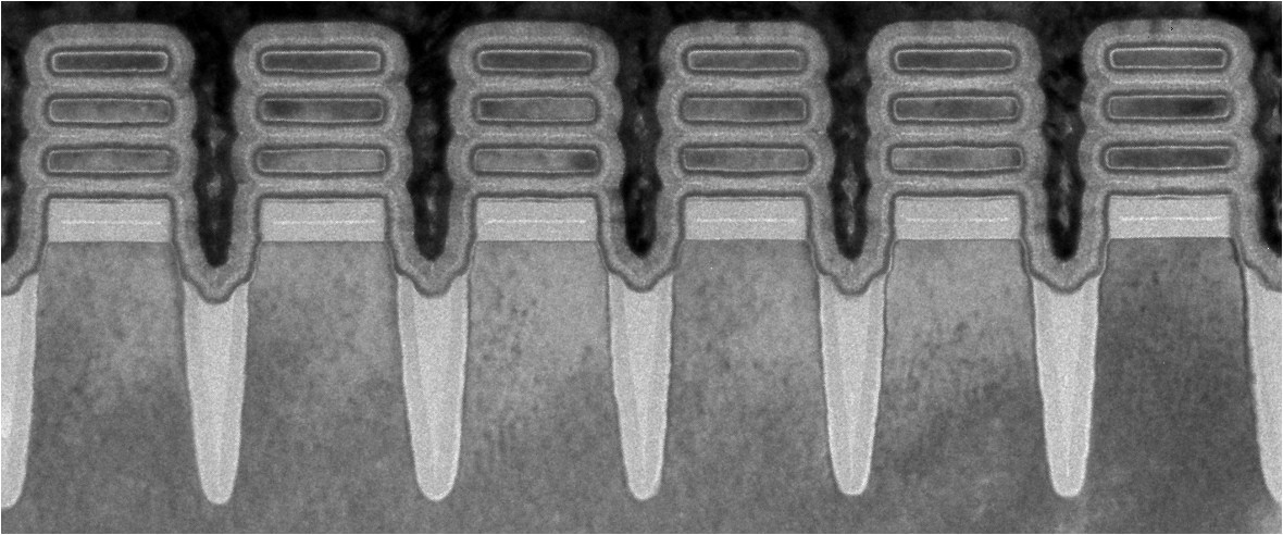
2 nm technology as seen using transmission electron microscopy. Courtesy of IBM.


 Animation, 3D Art and 3D Models")