Open side-bar Menu
 EDACafe Editorial

Archive for May, 2021

Higher density DRAM alternative; faster simulations; new chip prototyping program

Thursday, May 27th, 2021

Chip shortage and foundry activity continue to make headlines. Tesla is reportedly considering paying in advance for chips to secure its supply, and is said to be even exploring the acquisition of a semiconductor fab. GlobalFoundries is reportedly working with Morgan Stanley on an initial public offering that could value the foundry at about $30 billion. Let’s now move to some process technology and EDA updates.

Vertical nanowire-based memory promises 4X DRAM density without special materials

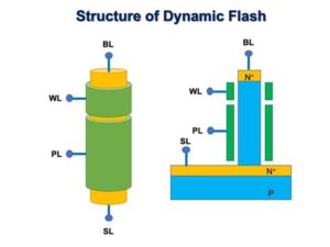
Singapore-based Unisantis unveiled the developments of its Dynamic Flash Memory (DFM) technology at the recent IEEE International Memory Workshop. According to the company, DFM offers faster speeds and higher density when compared to DRAM or other types of volatile memory. DFM is also a type of volatile memory, but since it does not rely on capacitors it has fewer leak paths, and it has no connection between switching transistors and a capacitor. The result is a cell design with the potential for significant increases in transistor density. Additionally – as it offers ‘block erase’ like a Flash memory – DFM reduces the frequency and the overhead of the refresh cycle and can deliver significant improvements in speed and power compared to DRAM. Based on TCAD simulation, Unisantis claims that DFM can potentially achieve a 4X density increase compared to DRAM. So, while the scaling of DRAM has almost stopped at 16Gb, DFM could be used to build 64Gb memory devices. Unisantis points out that unlike the so-called ‘emerging memory technologies’ (MRAM, ReRAM, FRAM, PCM), its Dynamic Flash Memory does not require using additional materials on top of a standard CMOS process. DFM was developed by Unisantis with the principles of its patented surround gate transistor (SGT) technology, also referred to in the semiconductor industry as a vertical nanowire transistor. According to the company, the benefits of this technology include improved area density, compared to planar and FinFET transistors; reduced leakage power, due to the strong electrostatic control of the surrounding gate to the transistor channel; and the possibility of optimizing the transistor width and length for different power/performance combinations. Unisantis is working on SGT technology in collaboration with Belgian research institute Imec.

DFM structure. Credit: Unisantis

(more…)

Chip lead times; Samsung EUV lines in Austin; Google 3D videoconferencing; data-driven algorithm design

Thursday, May 20th, 2021

Chip shortage and new fab plans continue to be hot topics this week, while there is no shortage of AI news – with Google announcing the next generation of TPUs, and Edge Impulse expressing an interesting concept about machine learning bound to replace code writing in algorithm design.

Chip lead times reach 17 weeks

According to a research by Susquehanna Financial Group, quoted by Bloomberg, chip lead times – the gap between order and delivery – increased to 17 weeks in April. That is the longest wait since the firm began tracking the data in 2017. Specific product categories reported even longer lead times: 23.7 weeks in April for power management chips, about four weeks more than a month earlier; industrial microcontrollers also showed a worsened situation, with order lead times extended by three weeks. Automotive chip supply continues to be a pain point, with NXP reportedly having lead times of more than 22 weeks now – up from around 12 weeks late last year – and STMicroelectronics to more than 28 weeks. This situation is raising concerns of ‘panic ordering’ that may lead to market distortions in the future.

(more…)

IBM’s 2nm chip; EDA updates; AI updates; acquisitions

Thursday, May 13th, 2021

Catching up on some of the news from the last four weeks or so, the IBM 2-nanometer announcement definitely stands out as a major update. Several recent news also concerns EDA, as well as AI accelerators. Two of the newest updates about AI startups will translate into an additional $150 million pumped into this industry by investors.

IBM’s 2-nanometer chip

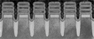
As widely reported by many media outlets, last May 6 IBM announced the development of the world’s first chip with 2-nanometer nanosheet technology. The result was achieved by IBM research lab located at the Albany Nanotech Complex in Albany, NY, where IBM scientists work in collaboration with public and private sector partners. According to the company, IBM’s new 2-nanometer chip technology will achieve 45 percent higher performance, or 75 percent lower energy use, than today’s most advanced 7-nanometer node chips. Reporting about the announcement, EETimes underlined that this chip is the first to use extreme-ultraviolet lithography (EUV) for front-end of line (FEOL) processes. Other details reported by EETimes include the use of bottom dielectric isolation to eliminates leakage current between nanosheets and the bulk wafer; and a novel multi-threshold-voltage scheme. Reportedly, IBM expects 2-nanometer foundry technology based on this work to go into production towards the end of 2024.

2 nm technology as seen using transmission electron microscopy. Courtesy of IBM.

(more…)

A closer look at Cadence’s new Palladium Z2 Enterprise Emulation and Protium X2 Enterprise Prototyping systems

Friday, May 7th, 2021

As gate count of advanced chips gets bigger and bigger, design teams need more powerful emulation and prototyping systems to reduce time-to-market. Cadence, for its part, is responding to this need with the introduction of its Palladium Z2 Enterprise Emulation and Protium X2 Enterprise Prototyping systems, the latest generation of a coordinated solution that the company has dubbed “Dynamic Duo”. Let’s now take a closer look at these two new systems with the help of Paul Cunningham, Senior Vice President, System & Verification Group at Cadence, who recently gave a video interview on this topic to Sanjay Gangal from EDACafe.

EDACafe interviews Paul Cunningham, Senior Vice President, System & Verification Group at Cadence

Doubled capacity, 50% performance increase

The key to improved performance and capacity – compared to the previous generation of these systems, Palladium Z1 and Protium X1 – is the adoption of new processing engines. “They are powered by two different chips,” Cunningham explained. “Palladium Z2 is powered by a custom ASIC we actually built here at Cadence, (…) and Protium X2 is based on a massive capacity, leading edge Xilinx FPGA, the VU19P.” As Cunningham pointed out, Cadence has built two entirely new platforms around these chips, with new rack and new boards, achieving significant results: “Within the same rack footprint [as the previous generation], we are doubling the capacity per rack and we are increasing the performance by 50%. So there’s a very significant uplift in both these platforms.”

(more…)


© 2024 Internet Business Systems, Inc.
670 Aberdeen Way, Milpitas, CA 95035
+1 (408) 882-6554 — Contact Us, or visit our other sites:
TechJobsCafe - Technical Jobs and Resumes EDACafe - Electronic Design Automation GISCafe - Geographical Information Services  MCADCafe - Mechanical Design and Engineering ShareCG - Share Computer Graphic (CG) Animation, 3D Art and 3D Models
  Privacy PolicyAdvertise