EDACafe Editorial Roberto Frazzoli
Roberto Frazzoli is a contributing editor to EDACafe. His interests as a technology journalist focus on the semiconductor ecosystem in all its aspects. Roberto started covering electronics in 1987. His weekly contribution to EDACafe started in early 2019. Vitis HLS now open source; an OS to manage SoC test; advancements in FD-SOI, EUV litho and DSA; AI chip updatesMarch 11th, 2021 by Roberto Frazzoli
Catching up on some of the news from the last couple of weeks or so, let’s start with a recent update concerning Apple: the company is reportedly planning to build a new semiconductor design center in Munich, Germany, as part of a 1 $1.2 billion investment push to develop custom chips for 5G mobile and other wireless technologies. According to the report, Apple plans to move into the facility in late 2022 and plans to hire hundreds of people. Xilinx Vitis HLS front-end is now open source Xilinx has made the decision of opening access to the front-end of Vitis HLS (high level synthesis) on GitHub. The Vitis HLS tool allows C, C++, and OpenCL functions to be deployed onto the device logic fabric and RAM/DSP blocks. Making the Vitis HLS front-end available on GitHub enables developers to tap into the technology and modify it for the specific needs of their applications.
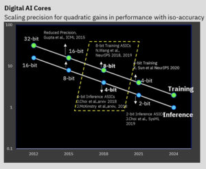
DARPA funds Julia Computing Julia Computing has been awarded funding by DARPA to accelerate simulation of analog and mixed-signal circuit models using machine learning and artificial intelligence techniques, with the goal of simulating these designs 1000x faster while maintaining acceptable levels of accuracy. The company has already used newly developed “surrogate architectures”, such as their Continuous Time Echo State Network (CTESN) architecture, to demonstrate acceleration in excess of 100x in multi-physics simulations. Based in Cambridge, MA, Julia Computing was founded in 2015 by the creators of the Julia language. An operating system for SoC test operations Breker has recently announced its “Synthesizable VerificationOS”, that allows operating system-like services to be automatically embedded in test content and manages the execution of concurrent test operations. “Modern SoCs require functional tests that can track the highly complex corner cases created by operational concurrency in both software and hardware,” notes Adnan Hamid, Breker’s CEO, in a press release. “Just like software needs an OS, software-driven test content requires the Synthesizable VerificationOS to simplify composition, scale concurrent coverage and drive shift-left test content portability.” According to the company, the solution is efficient enough to be executed during the simulation or emulation of an RTL design, saving hours of test composition while enabling a high degree of test portability from UVM to SoC and Post-Silicon environments. The Synthesizable VerificationOS integrates services which otherwise must be written manually; it also schedules concurrent test threads together with required resources and manages the entire verification process. Wave Computing and MIPS emerge from Chapter 11 and adopt the Risc-V standard Wave Computing and its subsidiaries including MIPS Tech have emerged from Chapter 11 bankruptcy protection. Going forward, the restructured business will be known as MIPS. The company is developing a new architecture which will be based on the open source Risc-V processor standard. New adaptive back-biasing architecture for FD-SOI chips boosts operating frequency by 450% French research Institute CEA-Leti and French company Dolphin Design have developed an adaptive back-biasing (ABB) architecture for FD-SOI chips that can be seamlessly integrated in the digital design flow with industrial-grade qualification. The new architecture, presented in a paper at ISSCC 2021, enables reducing energy consumption of processors in 22nm FD-SOI technology by up to 30 percent and increasing the operating frequency up to 450 percent compared to a technique in which body biased technique is not used. It also improves the manufacturing yield. According to the proponents, the new architecture is reusable for any biased digital load, and its IP adds a low overhead in terms of both area and power. EUV single patterning up to 28nm, directed self-assembly up to 18nm Papers presented by Belgian research center Imec at the 2021 SPIE Advanced Lithography Conference reported innovations for current and future process nodes. As for ‘traditional’ top-down lithography, Imec has demonstrated the ultimate single-exposure patterning capability of today’s 0.33NA (numerical aperture) EUV lithography equipment “NXE:3400”, built by Dutch company ASML. Process optimizations have enabled the patterning of dense 28nm pitch line/spaces with an Inpria metal-oxide resist in one single exposure, which corresponds to critical back-end-of-line metal layers of a 5nm technology node. Single-exposure clearly is less expensive and simpler that multi-patterning. Aiming at sub-2nm process nodes, Imec has also demonstrates for the first time the capability of directed self-assembly (DSA) to pattern line/spaces with a 18 nm pitch. As explained in this press release, the traditional top-down lithography patterning is increasingly challenged with issues that are inherent to the reaction of the photosensitive materials with light. DSA, instead, is a bottom-up approach that uses the microphase separation of a block copolymer (BCP) to define a pattern. The pattern can be engineered by tuning the composition and size of the polymer. The assembly can be further guided – directed – by using a prepattern of either line/spaces or holes. AI updates: IBM Research, ArchiTek IBM Research’s focus on low-precision training and inference as a way to boost AI energy efficiency has begun to bear fruit. In a paper presented at ISSCC 2021 (and summarized in this blog post), researchers introduced a 7-nanometer AI chip optimized for low-precision training and inference for all of the different AI model types — without any loss of quality at the application level. The chip is based on the innovations that IBM Research has developed over the past few years: namely, the use of 8-bit for training and 4-bits for inference, thanks to new algorithmic techniques that avoid loss of prediction accuracy, and through the development of an ultra-low precision hybrid FP8 (HFP8) data format. Other innovations implemented in the new chip include data communication protocols that enable AI cores on a multiple-core chip to exchange data effectively with each other; a power management function that slows down the chip during computation phases with high power consumption; and mechanisms to maximize utilization up to more than 80 percent for training and more than 60 percent for inference — whereas typical GPU utilizations are well below 30 percent. Japanese startup ArchiTek – founded in 2011, with US office in Menlo Park, CA – has recently announced its first AI acceleration chip for edge applications. Called “AiOnIc”, it is based on a proprietary architecture dubbed “ArchiTek Intelligence Pixel Engine” (aIPE). In a press release, the company claims “true high performance with extremely low power at a fraction of the price of GPUs”. The chip is manufactured in a 12 nanometer TSMC process, with a declared consumption of “under 1 Watt” and no need for a cooling fan. Qualcomm improves wireless audio The recently announced “Qualcomm Snapdragon Sound” is a solution mainly designed to improve wireless audio for earbuds and headsets – but also for smartphones and wireless gaming – supporting high-resolution 24-bit 96kHz audio and ultra-low latency. These results have been achieved through a system-level approach that aggregates multiple Qualcomm technologies and products, addressing both sides of the wireless link. Updates concerning Qualcomm include a comment about the company’s recent acquisition of CPU startup Nuvia. According to microprocessor analyst Linley Gwennap, the deal “indicates [Qualcomm’s] dissatisfaction with Arm’s CPU roadmap and its need for differentiated smartphone processors.” Events DVCon U.S. 2021 ran from March 1 to 4 as a virtual event, totaling 1,329 attendees who voted to select the following best papers: “Formal Verification Experiences: Spiral Refinement Methodology for Silicon Bug Hunt.”, by Siemens EDA; “Advanced UVM, Multi-interface, Reactive Stimulus Techniques,” by Paradigm Works and other companies; “Open-Source Framework for Co-Emulation Using PYNQ,” by Romanian company Amiq Consulting. IPC Apex Expo 2021 has started as a virtual event last March 9 and will run until March 12. The best paper selected by the conference’s Technical Program Committee is “Signal Integrity, Reliability, and Cost Evaluation of PCB Interlayer Crosstalk Reduction”, by IBM. Papers selected for the “honorable mention” are “Board Thickness Effect on Accelerated Thermal Cycle Reliability”, by Nokia and other companies; and “Analyzing Printed Circuit Board Voiding and other Anomalies when Requirements Covering the Anomalies are Vague”, by The Charles Stark Draper Laboratory. Upcoming virtual events include the tinyML Summit, which will be held the week of March 22, 2021; and the International Symposium on Quality Electronic Design (ISQED), from April 7 through Friday, April 9, 2021. |
|
|
|||||
|
|
|||||
|
|||||


