Microsoft has just announced it will permanently close all its retail stores around the world – except for four “Microsoft Experience Centers” in London, NYC, Sydney, and Redmond campus locations. The company’s retail team members will continue to serve customers from Microsoft corporate facilities and remotely. This was the biggest news today, but many other interesting things happened recently; some of them are summarized below.
Samsung launches its Cloud Design Platform
Last week EDACafe briefly reported about TSMC’s initiative aimed at using Microsoft Azure to speed up timing signoff for advanced-node SoC designs, with two separate collaboration agreements involving Cadence and Synopsys respectively. More cloud-based EDA news this week are coming from Samsung, that has launched its ‘Samsung Advanced Foundry Ecosystem (SAFE) Cloud Design Platform (CDP)’ for fabless customers, in collaboration with Rescale (San Francisco, CA). The two announcements are different in many respects: according to a press release, Samsung Foundry initiative is not focusing on timing signoff only but is offering a virtual “design environment” where customers can use tools from multiple vendors such as Ansys, Cadence, Mentor and Synopsys. Also, instead of collaborating with a single cloud service provider, Samsung Foundry has chosen Rescale’s multi-cloud platform. Rescale partners with several providers such as Amazon Web Service, Microsoft Azure, Google Cloud Platform, IBM, and Oracle Cloud Infrastructure. Common to both initiatives, obviously, is the goal of using cloud resources to speed up processing. Gaonchips – one of Samsung Foundry’s Design Solution Partners – has already tested the SAFE CDP on its 14nm automotive project using Cadence’s Innovus Implementation System and claims a 30 percent reduction of its design run-time compared to current on-premise execution times.
Mentor adds UltraSoC monitoring IP to its Tessent suite
Siemens, Mentor’s parent company, has signed an agreement to acquire UltraSoC (Cambridge,UK), a company providing a modular IP platform that allows to create on-chip monitoring and analytics infrastructures. UltraSoC’s IP is designed to accelerate silicon bring-up, optimize product performance, and confirm that devices are operating “as designed” for functional safety and cybersecurity purposes. Siemens plans to integrate UltraSoC’s technology into the Xcelerator portfolio as part of Mentor’s Tessent software product suite. Together with Tessent’s design-for-test (DFT) solutions, the combined offering is aimed at creating a ‘Design for Lifecycle Management’ solution for system-on-chips.
CMOS device fabrication at 500°C enables 3D monolithic integration
French research institute CEA-Leti is in the news again this week with another paper presented virtually during the 2020 Symposia on VLSI Technology & Circuits. The work, done in collaboration with Samsung, demonstrates the possibility of fabricating FDSOI CMOS devices without exceeding the 500°C temperature threshold. Conventional CMOS manufacturing processes require temperatures higher that 500°C, making it difficult to build 3D monolithic structures, since fabricating the upper-level transistors could damage the metal interconnects and the silicide of the bottom-level transistors. The low-temperature process developed by CEA-Leti for top-level devices prevents deterioration of bottom-level transistors, paving the way to 3D monolithic integration which promises many benefits over die stacking.
Arm-based Japanese supercomputer is number one in TOP500 list
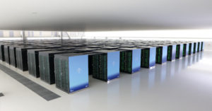
Called Fugaku, the most powerful supercomputer in the world is installed at Riken Center for Computational Science in Kobe, Japan. The machine, powered by Fujitsu’s A64FX processors containing forty-eight Arm cores, is number one in the latest TOP500 supercomputer list – the new edition of the ranking compiled twice a year by experts from Lawrence Berkeley National Laboratory, University of Tennessee Knoxville, and ISC Group (Frankfurt, Germany). With a High Performance Linpack (HPL) result of 415.5 petaflops, Fugaku dramatically outperforms number two on the list, an IBM-built supercomputer called Summit that delivers 148.8 petaflops on HPL. According to Riken Center, Fugaku also swept the competitors taking first place on three different rankings: the HPCG (High-Performance Conjugate Gradient) benchmark, based on real-world applications; HPL-AI, based on tasks typically used in artificial intelligence applications; and Graph 500, based on data-intensive loads. As underlined by Riken Center, this is the first time in history that the same supercomputer has become number one on these three rankings simultaneously. As usual, the TOP500 list provides many interesting insights. Only 144 systems – out of 500 – are using accelerators or coprocessors, the majority of which (135) are equipped with Nvidia GPUs. The x86 continues to be the dominant processor architecture, used by 481 of the 500 systems. Intel claims 469 of these, with AMD installed in 11 and Hygon in the remaining one. Arm processors are used by just four TOP500 systems, three of which employ the Fujitsu A64FX processor, with the remaining one powered by Marvell’s ThunderX2 processor. Chinese manufacturers lead the list in terms of number of installations with Lenovo (180), Sugon (68) and Inspur (64). The breakdown of system interconnect shows that Ethernet is used in 263 systems, InfiniBand in 150, and the remainder employ custom or proprietary networks.
Radar-based blood pressure measurement
Infineon’s Silicon Valley Innovation Center (SVIC), based in Milpitas, has entered in a new agreement with startup Blumio (San Mateo, CA) to co-develop a wearable, non-invasive blood pressure sensor based on Infineon’s XENSIV radar chipset by 2021. Key concept is using a radar sensor to detect the microscopic motions on the surface of the skin caused by pulsation traveling along the artery, then applying proprietary algorithms to extract blood pressure and other heart related metrics from the acquired waveform. According to the German chipmaker, the new sensor has the potential to disrupt the USD 45 billion market for wearable cardiovascular monitoring devices by enabling continuous and precise measurement without a cuff. In its incubator role, the SVIC will provide funding and resources to support the sensor’s commercialization.
Acquisitions
Besides the above-mentioned Siemens-UltraSoC deal, two more acquisition announcements are in the news this week. Preannounced last March, the pending acquisition of Adesto (Santa Clara, CA) by UK-based Dialog Semiconductor is expected to close on June 29, 2020, now that the parties have received the green light from the Committee on Foreign Investment in the United States. And Keysight has completed the acquisition of Eggplant – a software test automation platform provider – from The Carlyle Group.


