Advanced semiconductor technology is in the spotlight this week, with some significant innovations that have been presented at the 2020 Symposia on VLSI Technology and Circuits – a virtual event this year. More news concern power devices and embedded software; but first, a few EDA and FPGA updates.
Cloud-based timing signoff: TSMC, Microsoft, Cadence, Synopsys
Leveraging Microsoft Azure cloud computing to speed-up timing signoff for advanced-node SoC designs meant to be fabricated by TSMC: this is the goal of two separate three-way collaboration agreements, one involving Cadence and the other Synopsys. In the case of Cadence, the collaboration concerns the Tempus Timing Signoff Solution and the Quantus Extraction Solution, which customers will use with the Cadence CloudBurst Platform; for Synopsys, tools involved in the agreement are PrimeTime static timing analysis and StarRC parasitic extraction. Both Cadence and Synopsys cited massive parallelization and scalability – made possible by cloud computing – as the major benefits enabling a speed-up in timing signoff. White papers providing more details about these cloud-based solutions are available for TSMC customers in the foundry’s website.
Open source suite of development tools for QuickLogic FPGAs
With its QORC initiative (QuickLogic Open Reconfigurable Computing), QuickLogic claims to be the first programmable logic vendor to actively embrace a fully open source suite of development tools for its FPGA devices and eFPGA technology. The initial offering, developed by Antmicro (Sweden/Poland) in collaboration with QuickLogic and Google, supports QuickLogic’s EOS S3 low power voice and sensor processing MCU with embedded FPGA, and PolarPro 3E discrete FPGA family. The EOS S3 open source development tools suite includes FPGA development flow (SymbiFlow); SoC emulation (Renode); Zephyr real time operating system, running on the Arm Cortex-M4F; and QuickFeather development kit.
Seven-layer gate-all-around FET outperforms FinFETs
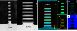
French research institute CEA-Leti has demonstrated fabrication of a new gate-all-around (GAA) nanosheet device as an alternative to FinFET technology targeting high-performance applications. Researchers have fabricated GAA nanosheet transistors with seven levels of stacked silicon channels, more than twice as many as state-of-the-art today. By increasing the number of stacked channels, CEA-Leti increased the effective width of the device for a given layout footprint, thus inducing higher drive current and achieving a better DC performance than leading-edge devices. CEA-Leti’s demonstration was based on a “replacement metal-gate” process developed for FinFETs.

First demonstration of GAA NanoSheet transistors with 7 stacked channels from tall and straight (SiGe/Si) fins (15nm≤W≤85nm). Copyright CEA-Leti
Tungsten buried power rails improve SRAM performance at 3 nanometers
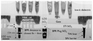
Belgian research institute Imec has demonstrated a tungsten buried power rail (BPR) integration scheme in a FinFET CMOS test vehicle, which does not adversely impact the CMOS device characteristics, showing excellent resistance values and electromigration behavior. A complementary study shows the advantages at system level of implementing BPRs as a scaling booster in 3 nanometer SRAM designs. As explained in a press release, buried power rails have recently emerged as an attractive structural scaling booster allowing a further reduction of standard cell height. Power rails are traditionally implemented in the chip’s back-end-of-line (BEOL); BPRs on the contrary are buried in the chip’s front-end-of-line (FEOL) to help free up routing resources for the interconnects. Integrating BPRs within the front-end module is however challenging, as BPR processing may induce stress in the conduction channel or cause metal contamination issues. Imec researchers avoided these problems by burying the W-BPR below the fin, deep into the shallow trench isolation (STI) module, and by capping the BPR metal by dielectric until the end of the processing. In a SRAM, moving the VDD and VSS power lines below the device allows more space for word- and bitline, offering a significant performance boost at system level. Imec simulations showed a 28.2% performance improvement for a server-processor having BPR-SRAMs with respect to conventional SRAM bit cells in L2 and L3 cache.
Voltage-controlled MRAMs gain higher write speed and better manufacturability
Imec has also solved two fundamental operation challenges which have so far limited the write speed and manufacturability of voltage-controlled magnetic anisotropy (VCMA) magnetic random access memories (MRAMs): the need for pre-reading the device before writing, and the need for an external magnetic field during switching. Briefly summarizing the explanation provided in this press release, the pre-read step has been avoided thanks to differentiated voltage thresholds for the two memory states; and the external magnetic field is no longer necessary thanks to a magnetic hardmask embedded on top of the magnetic tunnel junction. With these innovations, VCMA MRAMs fabricated using a 300mm state-of-the-art CMOS infrastructure can achieve nanosecond-scale speed and 20 femtojoule write energy, outperforming STT-MRAMs. According to Imec, VCMA MRAMs are now ideal candidates for high-performance, low-power and high-density memory applications.
Rohm lowers ON resistance for SiC MOSFETs
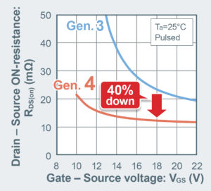
Rohm Semiconductor has announced the fourth generation of its 1200V SiC MOSFETs, claiming 40% lower ON resistance – while still maintaining short circuit withstand time – and 50% lower switching loss. The company has achieved these advancements over its previous generation SiC MOSFETs by improving their double trench structure and reducing their gate-drain capacitance. Bare chip samples of the new devices have been made available from June 2020, with discrete packages to be offered in the future.
“Mission critical edge” software bundles from Lynx
“Mission critical edge” is the expression coined by Lynx Software Technologies (San Jose, CA) to designate edge computing solutions that require robust system-safety mechanisms, state-of-the-art security, and real time determinism with sub-microsecond latency – such as the ones needed by industrial automation, drones, satellites, and avionics. Now Lynx is addressing this emerging market – which, according to the company, will have a $16 billion SAM in 2023 – with three new bundles based on MOSA.ic, its framework for development and integration of complex multicore safety or security systems. The three new bundles are targeted to industrial, UAVs/satellites, and avionics applications respectively. Built on the LynxSecure separation kernel hypervisor, MOSA.ic supports a variety of operating systems and runs on Intel, Arm and PowerPC processors.


