EDACafe Editorial Roberto Frazzoli
Roberto Frazzoli is a contributing editor to EDACafe. His interests as a technology journalist focus on the semiconductor ecosystem in all its aspects. Roberto started covering electronics in 1987. His weekly contribution to EDACafe started in early 2019. AV standards and simulation; carbon nanotube transistors; gallium oxide MOSFETs; RISC-V IP in FPGA designsJune 5th, 2020 by Roberto Frazzoli
Autonomous vehicles obviously continue to be a hot theme, both in terms of business – with Amazon reportedly in advanced talks to buy self-driving car tech company Zoox (Foster City, CA) – and in terms of technology. Recent AV tech updates include a new standard and improved simulation solutions. More news this week come from academic research on new materials, both for IT and for power applications; lastly, one more FPGA vendor offering simplified solutions for non-expert designers. Autonomous vehicles updates: UL 4600 standard, news from AVSimulation and Foretellix The amount of technical standards specifically addressing autonomous vehicles is growing: last week we briefly reported about IEEE 2846, a “formal model for safety considerations in automated vehicle decision making”; and last April 1 Underwriters Laboratories announced the publication of UL 4600, a “standard for safety for the evaluation of autonomous products”.
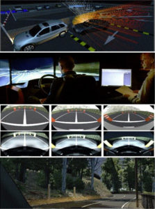
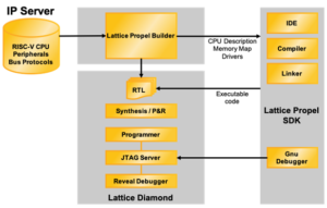
A key role in the development of UL 4600 was played by Dr. Philip Koopman of Edge Case Research, a specialized company based in Pittsburgh, PA, whose website contains a page with links to webinars and other specific resources concerning this standard. As explained by Edge Case Research, UL 4600 focuses on questions such as “Did you do enough?” and “Did you think of that?” Examples of issues that should be taken into account when designing a “safety case” include sun angle changes, seasonal events (e.g., Oktoberfest), presence of snowplows, sand/salt trucks, police vehicles intentionally blocking traffic, post-collision vehicles and associate debris, and many, many more. In terms of “Did you think of that?”, other interesting examples of how challenging AV safety can be come from the recently announced update of the simulation platform offered by French company AVSimulation: additional features of the new SCANeR studio can now address defects and details on the road – such as cracks, tire marks, road repairs – and composite road signs consisting of two signs on the same pole. Both above-mentioned companies, Edge Case Research and AVSimulation, are collaborating with Ansys (details can be found here and here), which in a recent blog post has reiterated the importance of road testing simulation for the advancement of autonomous vehicles. Ansys standpoint on this topic can be found in this video featuring Walt Hearn, VP Americas. According to Ansys, what makes simulation essential is the enormous amount of real road testing that would otherwise be required to ensure safety: 8.8 billion miles – based on a Toyota estimation dating back to 2016. Also addressing AV testing – with a coverage-driven approach borrowed from the semiconductor industry – is Israel-based startup Foretellix, that has recently announced a new integrated workflow connecting its Foretify platform with the Virtual Test Drive (VTD) simulation software provided by Germany-based Vires. Foretellix aims to enable ‘measurable safety’ of autonomous vehicles, moving from ‘quantity of miles’ to ‘quality of coverage’. To this goal, the company has adapted a “highly automated and proven” coverage-driven methodology broadly adopted in the semiconductor industry. Foretellix’s Foretify Technology includes an open, high-level “Measurable Scenario Description Language” (M-SDL), automation, analytics and metrics. Carbon nanotube transistors get closer to real world applications A team of MIT researchers has demonstrated that carbon nanotube transistors (CNFETs) can be fabricated in large quantities on regular 200-millimeter wafers, opening a path for this technology to move from academic lab to commercial applications. The researchers worked with Analog Devices and SkyWater Technology (Bloomington, MN), a semiconductor foundry. Key to the new manufacturing process was a dramatic speed-up of the deposition phase (called “incubation”) where a wafer is submerged in a bath of nanotubes until they stick to its surface. Using dry cycling, a method of intermittently drying out the submerged wafer, the incubation time was reduced from 48 hours to 150 seconds. The incubation method doesn’t allow to align the nanotubes, which would be necessary to obtain ideal CNFET performance; however, the researchers concluded that CNFETs can outperform silicon-based transistors even without nanotube alignment. According to the MIT team, benefits of CNFETs include higher energy efficiency and a lower temperature manufacturing process. This would allow to build 3D chips by adding circuit layers without melting the layers underneath. Gallium oxide power transistors achieve 8 kilovolt breakdown voltage Researchers from University at Buffalo (Buffalo, New York) have fabricated gallium oxide (Ga2O3) power transistors that achieve a maximum breakdown voltage of 8.03 kV. The field plated lateral MOSFETs reached this performance thanks to polymer passivation – with the addition of a layer of SU-8, an epoxy-based polymer. According to the research team, the passivation layer is a simple, efficient and cost-effective way to boost the performance of gallium oxide transistors – making them even more competitive against silicon carbide or gallium nitride devices. Gallium oxide’s bandgap is about 4.8 electron volts, which places it in the ultrawide bandgap group of materials. Silicon carbide and gallium nitride bandgaps are about 3.4 electron volts and 3.3 electron volts respectively. Drag-and-drop IP blocks in your FPGA design Making FPGAs easier to use for all designers is clearly a key concern in the FPGA industry nowadays. In different forms, this concept applies to Xilinx’ Vitis, Intel’s oneAPI, and Microchip’s VectorBlox; now Lattice joins the group with its new software solution Propel, designed to accelerate development of its low power FPGAs. According to the company, Propel will empower developers of “any skill level” to quickly and easily design Lattice FPGA-based applications by enabling the easy assembly of components from an IP library that includes a RISC-V processor core and numerous peripherals. As highlighted in a press release, “For novice FPGA developers, the Lattice Propel GUI simplifies the design process by enabling them to drag-and-drop IP blocks from the Lattice IP library into their designs.” Lattice claims to be the first supplier of SRAM and Flash-based FPGAs to provide access to RISC-V technology in a simple drag-and-drop system builder environment. |
|
|
|||||
|
|
|||||
|
|||||


