EDACafe Editorial Roberto Frazzoli
Roberto Frazzoli is a contributing editor to EDACafe. His interests as a technology journalist focus on the semiconductor ecosystem in all its aspects. Roberto started covering electronics in 1987. His weekly contribution to EDACafe started in early 2019. ASML results; epitaxy market; microdisplays; universal memory; perfect secrecy; NoCs in FPGAs; photonics eventsJanuary 24th, 2020 by Roberto Frazzoli
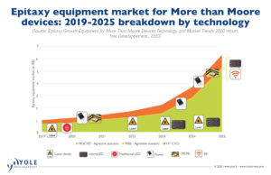
Equipment, materials and processes are in the spotlight this week – but innovative algorithms and architectures deserve their share of attention, too. Strong EUV demand drives ASML growth Several years in the making, EUV lithography is now paying off for ASML. Fourth-quarter and full-year results just announced by the Dutch equipment manufacturer look very good: Q4 2019 net sales totaled €4.0 billion, with net income of €1.1 billion and gross margin of 48.1%. As for full 2019 results, net sales amounted to €11.8 billion with net income of €2.6 billion. For the first quarter of 2020, ASML expects net sales of between €3.1 billion and €3.3 billion and a gross margin between 46% and 47%. “We shipped eight EUV systems in the fourth quarter and we received orders for nine EUV systems,” said ASML’s CEO Peter Wennink in a statement. “We expect that 2020 will be another growth year, both in sales and in profitability, driven by EUV demand and our Installed Base business. The Logic market is expected to remain strong in 2020, due to investments in 5G and high-performance compute applications. In the Memory market, our customers are starting to see the first signs of recovery,” Wennink added. Epitaxy equipment market to expand Market expansion is forecasted for epitaxy equipment as well. According to French market research firm Yole Développement, the epitaxy growth equipment market for “More than Moore” devices was worth close to US$940 million in 2019 and it is expected to reach more than US$6 billion by 2025 in the “aggressive scenario” (one of the different possible market scenarios). Silicon substrates are by far the most dominant today with more than 80% market share, but alternative non-silicon-based substrates like GaAs, GaN, SiC and InP are gaining momentum within the “More than Moore” industry. GaN material represents the major epitaxy market after silicon substrates, mostly driven by the traditional LED GaN-devices. Factors expected to shape the epitaxy equipment market in the future include a stronger demand for VCSELs, miniLEDs and microLEDs, for SiC-based power devices, and for GaAs in 5G RF products. Technological advancements will be required for microLED epitaxy to further reduce the defect rate. One of the major factors prompting Yole to consider different growth scenarios is the potential impact of the decisions that the Chinese government could make to prevent GaN-based LED overcapacity build-up. AR microdisplays from Micledi and Mojo Vision MicroLEDs are indeed a hot topic these days, and a spinoff of Belgian research center Imec has recently raised 4,5M euro seed capital to develop microLED displays for next generation Augmented Reality glasses. Micledi, this is the name of the company, sets off to enable AR glasses that are “small, lightweight, with long battery life, and at reasonable cost”. To make this happen, the company is developing “the world smallest and brightest displays”- 100x brighter than commercial alternatives – using a new integration technology on 300mm wafers. And “the world’s densest microdisplay” is at the heart of one of the CES announcements that got the most press coverage this year: the augmented reality contact lenses being developed by Mojo Vision (Saratoga, CA). The concept is clear and compelling: a contact lens with a built-in display that projects information – such as walking directions, machine repair instructions etc. – directly onto your retina. New candidate for the role of universal memory Fast as a DRAM, non-volatile as a flash: the quest for the ‘universal memory’ doesn’t stop. Researchers at Lancaster University (UK) have come up with a new promising candidate: a compound-semiconductor charge-storage memory that exploits a quantum effect, resonant tunnelling. Simulations show that the device consumes very little power, with 100 times lower switching energy per unit area than DRAM, but with similar operating speeds. Nonvolatility is achieved due to the extraordinary band offsets of indium arsenide (InAs) and aluminium antimonide (AlSb), providing a large energy barrier (2.1 eV), which prevents the escape of electrons. New cryptography claiming perfect secrecy A research team with members from KAUST (King Abdullah University of Science and Technology, Saudi Arabia), the University of St Andrews (Scotland) and the Center for Unconventional Processes of Sciences (California) have devised what they claim is a “a perfect secrecy cryptography”, working in classical optical channels. The system exploits correlated chaotic wavepackets, which are mixed in inexpensive and CMOS compatible silicon chips. The chips can generate 0.1 Tbit of different keys for every mm of length of the input channel, and require the transmission of an amount of data that can be as small as 1/1000 of the message’s length. According to the research team, this scheme is protected against any possible attack by the second law of thermodynamics and the “exponential sensitivity of chaos”. Adding a NoC to an FPGA architecture The architecture of Achronix’s Speedster7t FPGA includes a network-on-chip. A white paper recently published by the company describes the benefits offered by this innovation. According to Achronix, traditional bit-wise routing in FPGAs is very flexible, but it has downsides: it adds delay to any given signal path – making timing closure difficult to achieve – and can incur congestion. With the rise of high-speed communication standards, a NoC connecting all of the on-chip high-speed interfaces – ports of 400G Ethernet, PCIe Gen5, GDDR6 and DDR4/5 – allows a number of benefits both in terms of performance and design process. Raymond Nijssen from Achronix will be chairing a panel at the upcoming FGPA 2020 event (ACM/SIGDA International Symposium on Field-Programmable Gate Arrays), scheduled for February 23 – 25 in Seaside, California. Panel theme: “FPGAs will never be the same again: How the newest FPGA architectures are totally disrupting the entire FPGA ecosystem as we know.” More news in brief Apple has reportedly acquired Seattle-based Xnor.ai, an AI startup specializing in low-power, edge-based image recognition tools. Synopsys has joined the Autonomous Vehicle Computing Consortium. Intel has joined CHIPS Alliance to promote Advanced Interface Bus (AIB) as an open-source, royalty-free PHY-level standard for connecting multiple semiconductor die – e.g. chiplets – within the same package. Photonics on show Photonics West, the event organized by Spie, will take place in San Francisco, at the Moscone Center, from February 1st to 6th. The conference will also feature a startup challenge in the healthcare and deep tech technology areas. Almost co-located – just a couple blocks away, at the San Francisco Marriott, on February 3rd – will be the ITF Photonics event organized by Belgian research center Imec. |
|
|
|||||
|
|
|||||
|
|||||


