


Another tech giant joins the AI race: Sony Corp. has reportedly launched Sony AI, a new R&D organization focusing on artificial intelligence. And AI is the major factor behind most of the recent news concerning processors of any kind. Many of these announcements came from the SC19 event (International Conference for High Performance Computing, Networking, Storage, and Analysis) recently held in Denver, CO.
Nvidia enables GPU-accelerated Arm-based servers
“Just a few years ago, an Arm-based HPC was difficult to fathom for many. Today, Arm is becoming established as the compelling platform for AI and HPC innovation to build upon.” This website post from Chris Bergey, SVP & GM of the Infrastructure Line of Business at Arm, explains why adding GPU acceleration to Arm architectures is now a hot topic. Earlier this year Nvidia announced that it will bring its Cuda-X software platform to Arm; now the GPU leader is introducing a reference design platform – consisting of hardware and software building blocks – to quickly build GPU-accelerated Arm-based servers for high performance computing applications. As a result, supercomputing centers, hyperscale-cloud operators and enterprises will soon be able to combine Nvidia’s accelerated computing platform with the latest Arm-based server platforms.
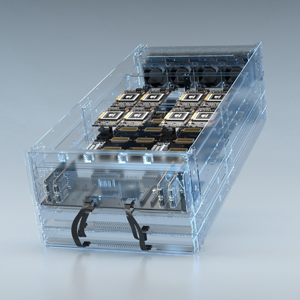
Nvidia reference design platform for GPU-accelerated Arm servers. Image credit: Nvidia
New GPUs from Intel
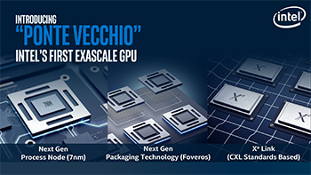
Ponte Vecchio (the Italian for ‘old bridge’, and the name of a famous Florence landmark) is the code name of a new category of Intel’s discrete general-purpose GPUs based on the company’s Xe architecture. The new GPUs are designed for HPC modeling, simulation workloads and AI training. Ponte Vecchio will be manufactured on Intel’s 7nm technology and will leverage Intel’s Foveros 3D and EMIB packaging innovations. It will also feature multiple technologies in-package, including high-bandwidth memory and Compute Express Link interconnect.
A new challenger in the datacenter processor market
With so many startups addressing AI acceleration, the announcement of a startup focusing on ‘regular’ datacenter processors sounds interesting. Even more so if the startup plans to compete directly against the datacenter market leader, Intel. This is, reportedly, the case of Nuvia, a company based in Santa Clara, CA, and led by industry veterans. The startup sets out with “the goal of reimagining silicon design to deliver industry-leading performance and energy efficiency for the data center.” According to Nuvia, achieving this target will require “a step-function increase in compute performance and power efficiency.” As of today, the company has not released any details about its future products. The company has recently closed its Series A funding round raising $53 million. Investors include Capricorn Investment Group, Dell Technologies Capital, Mayfield, WRVI Capital and Nepenthe LLC.
![]()
Startup bets on native graph processing
Formerly known as Thinci, the AI acceleration startup Blaize has emerged from stealth and introduced its “graph-native” proprietary SoCs, along with a software development platform. This approach is based on the assumption that “all neural networks are graphs”, as explained in a press release. According to Blaize, its Graph Streaming Processor (GSP) architecture enables concurrent execution of multiple neural networks and entire workflows on a single system. The architecture uses a data streaming mechanism where non-computational data movement is minimized or eliminated, thus reducing latency, memory requirements and energy demand. Non-neural network functions such as image signal processing can also be integrated and represented as graphs, thus achieving a 10-100x boost in processing efficiency. Supported by a US$87M funding from strategic and venture investors, Blaize claims engagements of early access customer since 2018 in automotive, smart vision and enterprise computing segments.
Combining x86 cores and AI coprocessor
Definitely not a startup, having been founded in 1995, Austin-based Centaur Technology is also taking part in the AI acceleration race with an SoC that combines eight new server-class x86 CPU cores with a 20 TOPS coprocessor optimized for inference applications in server, cloud and edge products. This unique approach is targeted at applications that require both x86 compatibility and AI acceleration, offering the benefits of integration compared to using an off-chip accelerator. Benefits cited by the company include lower cost, lower power, higher performance, and the possibility to avoid the use of specialized software tools. Eliminating the need to move data to an off-chip accelerator yields extremely low latency on inference tasks, as demonstrated by MLPerf benchmarks. Centaur Technology submitted audited results for four MLPerf inference applications in the Closed/Preview category, obtaining the fastest latency score of all submitters for image classifier benchmark Mobilenet-V1. Additionally, as stated in a Centaur press release, the company was the only chip vendor to submit scores for GNMT translation from English to German.
More AI chips news
More AI chips made news over the past couple of weeks. Graphcore’s Colossus GC2 was the subject of a Mentor announcement revealing that this 23.6 billion transistors chip was verified using Mentor’s Questa RTL simulation flow, in conjunction with Questa Verification IP solution for PCI Express. Gyrfalcon introduced its new Lightspeeur 5801 AI accelerator, highlighting its power efficiency for edge applications. With 2.8 TOPS of performance and using only 224 mW of power, the Lightspeeur 5801 achieves a 12.6 TOPS/W ratio.

Getting rid of lithography?
After so many processor announcements, let’s finish with some news from academic research in nanotechnology. What if crystal structures in electronic devices could be synthesized with the desired shape without using lithography and etching? A team of researchers from Johns Hopkins University have shown that this is possible – at least for certain transition-metal dichalcogenide (TMD) crystals – using a method that involves pre-treating the silicon surface with phosphine. With this technology, the team has built MoS2 (molybdenum disulfide) ‘nanoribbons’ and was able to control the width of these structures between 50 and 430 nanometers by varying the total phosphine dosage during the surface treatment step. Potential applications cited by the researchers include optoelectronic devices, energy storage, quantum computing and quantum cryptography.


 Animation, 3D Art and 3D Models")