


EDACafe Editorial Roberto Frazzoli
Roberto Frazzoli is a contributing editor to EDACafe. His interests as a technology journalist focus on the semiconductor ecosystem in all its aspects. Roberto started covering electronics in 1987. His weekly contribution to EDACafe started in early 2019. IR drop analysis; die-to-die connectivity; testing AV chips; ADAS devices and more weekly newsNovember 15th, 2019 by Roberto Frazzoli
Several interesting announcements are making news this week, both from EDA-IP vendors addressing the requirements of next generation chips, and from chipmakers targeting advanced automotive, consumer and industrial applications. Addressing the IR drop analysis issues Due to the effects of highly resistive lower metal layers, one of the challenges posed by the design of advanced high-speed chips at 7 nanometers and below concerns the IR drop analysis. In these designs, timing is dependent on IR drop and vice-versa, making IR drop analysis a key signoff technology. To address these issues, Cadence has integrated two of its preexisting products: the Tempus Timing Signoff Solution and the Voltus IC Power Integrity Solution. According to Cadence, the resulting tool – called Tempus Power Integrity Solution – allows to significantly lower IR drop design margins without sacrificing signoff quality, thus improving power and area. Early use cases cited by Cadence demonstrated that the new solution correctly identified IR drop errors, avoiding silicon failure prior to tapeout and improving the maximum frequency in silicon by up to 10%. Other benefits include a proprietary vectorless-based algorithm to identify critical paths most likely impacted by IR drop.
High speed die-to-die IP for chiplet-based and SiP devices Also from Cadence, a new IP for die-to-die connectivity in chiplet-based and System-in-Package devices targeted at high performance applications – such as AI/ML, 5G, cloud computing and networking. Called UltraLink D2D PHY IP, it delivers up to 40Gbps wire speed in an NRZ serial interface, providing up to 1Tbps/mm unidirectional bandwidth. The IP includes built-in de-skew and scrambling/de-scrambling logic to facilitate system integration, and requires only 28 data wires for 1Tbps bandwidth to simplify routing. As stressed by Cadence, the UltraLink D2D PHY IP supports multi-chip modules on organic substrates, a cheaper package option compared to other die-to-die solutions that require a silicon interposer. Proven in a 7nm FinFET process, the new Cadence IP features a 5ns latency round trip from receiver to transmitter and achieves better than 10-15 bit error rate without requiring forward error correction. 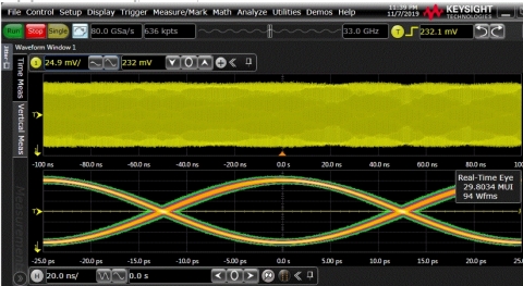 Cadence UltraLink D2D PHY IP 40G Transmit Eye. Image credit: Business Wire Meeting the test requirements of AV chips Automotive safety standard ISO 26262 takes into account a parameter called Fault Tolerant Time Interval (FTTI), the time period from the occurrence of a fault to the violation of a Safety Goal (SG). Assessing this parameter is just an example of the new test requirements posed by the chips targeted at autonomous vehicles. The designers of these advanced devices can now rely on the new Tessent software Safety ecosystem introduced by Mentor, a portfolio of automotive IC test solutions from both Mentor and its partners. Tessent Safety ecosystem leverages the automotive IP portfolio of Arm as part of the company’s Functional Safety Partnership Program. The ecosystem includes new BIST solution delivering up to 10x faster in-system test than traditional offerings. New ADAS and autonomous driving SoCs And speaking of advanced automotive chips, Xilinx has added two new devices to the XA Zynq UltraScale+ portfolio of MPSoC (multiprocessor system-on-chip), targeting ADAS and autonomous driving applications ranging from L2+ to L4. Called 7EV and 11EG respectively, these parts offer over 650,000 programmable logic cells and nearly 3,000 DSP slices, which is a 2.5X increase versus the previous largest device. In addition, the XA 7EV contains a video codec unit for h.264/h.265 encode and decode, while the XA 11EG includes 32 12.5Gb/s transceivers and provides four PCIe Gen3x16 blocks. The XA Zynq UltraScale+ MPSoC portfolio is AEC-Q100 qualified and integrates both Xilinx programmable logic and an ASIL-C-certified multicore processing system (quad-core Arm Cortex-A53 and dual-core Arm Cortex-R5).
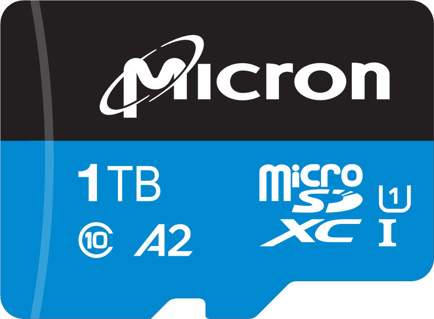
Ultra-wideband enables handsfree smartphone car access Waiting for future autonomous vehicles to become a reality, drivers will soon be able to open and start cars while leaving their phones in their pockets or bags – thanks to a new ultra-wideband chip announced by NXP, the NCJ29D5. The technology is designed to give ‘spatial awareness’ to UWB-equipped cars, mobiles, and other smart devices, to enable cars to know exactly where the users are. Other automotive UWB use cases targeted by the new NXP chip include easy trunk access, smartphone valet parking, drive-through payment and garage access. NXP, BMW, Continental and others are collaborating on this technology through the Car Connectivity Consortium (CCC) and IEEE, aiming to enable a global standard for handsfree smart access and other automotive localization use cases based on UWB. 8K TV sets getting closer to the market The new AI-equipped 8K TV system-on-chip jointly announced by MediaTek and TSMC has just entered volume manufacturing. Built with the foundry’s 12nm FinFET Compact (12FFC) technology, the MediaTek S900 integrates a proprietary AI processor supporting a variety of features, including voice recognition, facial recognition and scene recognition. The latter feature will enable S900-powered TVs to improve picture quality by optimizing color saturation, brightness, sharpness, and dynamic motion compensation. On the other hand, AI-powered voice or gesture recognition will allow these future TV sets to send commands to other smart devices in the living room, kitchen or bedroom. A way for TV sets to compete against refrigerators in the battle to conquer the role of central hub in future smart homes. The 1TB industrial-grade microSD card Besides AI processing capabilities, edge devices such as surveillance cameras are also gaining bigger memory capacities with 1TB microSD cards now available in the industrial-grade version. Micron Technology has just unveiled the first device of this kind, the i3001TB3 microSDXC UHS-I, to address the edge storage needs of the video surveillance market and other industrial applications. Based on Micron’s 96-layer 3D quad-level cell (QLC) NAND technology, the new card makes it cheaper for small- to medium-sized deployments to have primary storage in the camera compared to a centralized storage architecture. In a video surveillance camera, a single 1TB microSD card can store more than three months of high-quality video footage.
Semi capex concentration According to a report from IC Insights, the share of semiconductor industry capital spending held by the top five companies (Samsung, Intel, TSMC, SK Hynix, and Micron) is forecast to reach an all-time high of 68% this year. Samsung’s combined 2017, 2018, and 2019 capital expenditures for its semiconductor group are expected to be $65.8 billion, 53% more than Intel, the next highest spender over this same time period.
|
|
|
|||||
|
|
|||||
|
|||||


 Animation, 3D Art and 3D Models")