EDACafe Editorial Roberto Frazzoli
Roberto Frazzoli is a contributing editor to EDACafe. His interests as a technology journalist focus on the semiconductor ecosystem in all its aspects. Roberto started covering electronics in 1987. His weekly contribution to EDACafe started in early 2019. Major stories this week: wafer and chip sales; EDA on cloud; ARM vs open source; computer vision; additive manufacturingMay 3rd, 2019 by Roberto Frazzoli
First quarter results confirm the expectation of “headwinds” expressed by SEMI at a recent event. Second quarter now starts with many hot topics and promising innovations – from design to manufacturing. Wafer and chip sales down in Q1 2019 According to the SEMI Silicon Manufacturers Group, worldwide silicon wafer area shipments dropped 5.6 percent during the first quarter of 2019 compared to the fourth quarter of 2018 and are now at their lowest level since the fourth quarter of 2017. A bigger downturn has been reported by the Semiconductor Industry Association (SIA): worldwide sales of semiconductors totalled $96.8 billion during the first quarter of 2019, a decrease of 15.5 percent over the previous quarter and 13 percent less than the first quarter of 2018. Global sales for the month of March 2019 were $32.3 billion, a dip of 1.8 percent compared to the previous month's total and 13 percent less than sales from March 2018.
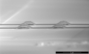
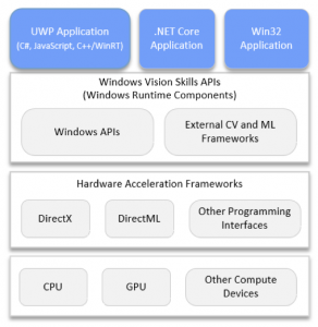
EDA on cloud expands TSMC has announced the expansion of its Open Innovation Platform (OIP) Cloud Alliance, with Mentor joining inaugural members Amazon Web Services, Cadence, Microsoft Azure, and Synopsys. Cloud Alliance is an initiative aimed to certifying that the capabilities of traditional EDA design flows can be utilized via the cloud. The first Mentor solution validated by TSMC is the Calibre physical verification tool: through a joint project involving Microsoft Azure, a 5nm test chip from TSMC took less than four hours to complete its verification thanks to the productivity boost enabled by Calibre in the cloud. The Cloud Alliance also gains another solution with the Cadence CloudBurst Platform, which enables customers to select critical parts of their EDA workload to deploy to the cloud, based on project needs. It enables a ready-to-use hybrid cloud environment running on Amazon Web Services (AWS) or Microsoft Azure. Also playing a role in cloud-based EDA is Google: eSilicon – a provider of FinFET ASICs, IP platforms and 2.5D packaging solutions – has announced an agreement with Google Cloud to move all of its ASIC and IP design to Google Cloud Platform (GCP) this calendar year. eSilicon has been running a hybrid on-premise/cloud environment for the last 18 months, with ASIC design running on premise and IP design running primarily on GCP. This new agreement paves the way for a complete migration of all design activity to GCP. Cloud computing for EDA will also be a theme at the upcoming Design Automation Conference in Las Vegas, June 2nd to 6th, which will be featuring a ‘Design-on-Cloud Pavilion’. ARM vs open source ISAs A new white paper by Linley Gwennap, Principal Analyst at The Linley Group, compares the ARM ecosystem with the tools and support offered by open source ISAs. “A low-cost unconstrained environment is good for research and some small chip developers”, Gwennap writes in his conclusion, referring to open source ISAs. “But for most commercial SoC projects, CPU license fees are a small portion of the design budget. Choosing a CPU with low or no license fees can create hidden costs—such as creating verification models, tool flows, and library code—that more than offset the reduction in up-front fees. Furthermore, any schedule delays caused by buggy RTL, physical-level redesign, or software problems could cost millions of dollars in missed market opportunities. Before putting an important SoC product at risk, consider the potential cost of a free ISA”, Gwennap concludes. ARM sponsored this white paper, but the opinions and analysis are those of Linley Gwennap. An eye on computer vision Microsoft has announced the preview of Windows Vision Skills, a set of NuGet packages that make it easy for application developers to solve complex computer vision problems using a simple set of APIs. With Windows Vision Skills, an app developer can use out-of-box WinRT APIs to add prebuilt vision skills like object detection, skeletal detection and face sentiment analysis in their Windows applications (.NET, Win32, and UWP); and a computer vision developer can leverage hardware acceleration frameworks on Windows devices by packaging his solution as a Vision Skill – without worrying about low-level APIs. Computer vision will take center stage at the upcoming Embedded Vision Summit (May 20-23, 2019, Santa Clara, California). Highlights of the program include keynotes from Google's Pete Warden and MIT's Ramesh Raskar, more than 90 other speakers, training sessions, and a start-up competition. This year's finalists are Blink.AI Technologies, Entropix, Robotic Materials, Strayos and Vyrill. Additive manufacturing adds new solutions Up to now, a weak point of additive manufacturing has been the realization of metallic structures at the micrometre scale. A team of researchers at ETH Zurich (Switzerland) have now developed an “electrohydrodynamic redox printing technique” that allows to print metals with a spatial resolution of 250 nanometres. To overcome the disadvantages of ink-based methods, the new technology uses metal ions created by applying an electric voltage to a ‘sacrificial anode’ consisting of the desired metal inside the printing nozzle. The ions, in a solvent, are then sprayed by electric forces onto the printing surface, where they lose their electric charge and reassemble as a metal. With a printing speed of ten voxels per second (a voxel is a volume element, similarly to a pixel in 2D printing), the technique can print two metals simultaneously or in alternation, by using two different sacrificial anodes – for example copper and silver. Additive manufacturing of PCBs, on the other hand, promises to shorten the design and development phase of new systems. Nano Dimension, an Israeli additive electronics provider, has announced that the company's DragonFly Pro systems have successfully shortened and simplified the assembly process for ball grid arrays (BGAs) and other surface mount technology components, from days to one hour. With a special layout structure achieved through additive manufacturing of PCBs, there is no need for special tooling for assembly. This enables in-house manual assembly of BGAs and SMT components during the design and application development phase. According to Nano Dimension, this means that system companies can do everything in-house, with no need for outside contractors and less risk of errors.  Silver stripes realized with electrohydrodynamic redox printing technique. Image credit: Alain Reiser / ETH Zurich Category: EDACafe Editorial |
|
|
|||||
|
|
|||||
|
|||||


