


EDACafe Editorial Roberto Frazzoli
Roberto Frazzoli is a contributing editor to EDACafe. His interests as a technology journalist focus on the semiconductor ecosystem in all its aspects. Roberto started covering electronics in 1987. His weekly contribution to EDACafe started in early 2019. Major stories this week: EDA industry updates; acquisitions; CNN training; MEMS; sensorless detection; drone deliveryApril 25th, 2019 by Roberto Frazzoli
The EDA industry is in good shape: according to a report from Reportlinker, the Electronic Design Automation market is expected to grow at a CAGR of 12.0% over the next eight years, reaching US$28.27 billion by 2027. Recent industry news include TSMC granting certifications for its System-on-Integrated-Chips stacking technology (TSMC-SoIC) to Ansys, Cadence, Mentor and Synopsys. Microsoft and Intel acquiring specialized companies IoT and AI are the two drivers behind the recent acquisitions from Microsoft and Intel respectively. The software giant has acquired Express Logic, a leader in real time operating systems (RTOS) for IoT and edge devices powered by microcontrollers. Express Logic’s ThreadX RTOS has over 6.2 billion deployments, making it one of the most deployed RTOS in the world. With this acquisition, Microsoft aims to grow the number of devices connected to its cloud computing service Azure and will enable new intelligent capabilities. Microsoft’s goal is to make Express Logic’s ThreadX RTOS available as an option for real time processing requirements on an Azure Sphere device and enable ThreadX-powered devices to connect to Azure IoT Edge devices when the IoT solution calls for edge computing capabilities. Intel has acquired Omnitek, a UK-based provider of video and vision FPGA IP solutions. Omnitek’s technology is clearly a complement to Intel’s FPGA business: last week, for example, Omnitek announced availability of a new Convolutional Neural Network optimized for the Intel Arria 10 GX architecture, claiming world-leading performance per watt (135 GOPS/W) at full 32-bit floating point accuracy. The design employs a new framework combining fixed point and floating point maths.
Google’s “visual” approach to speech recognition training 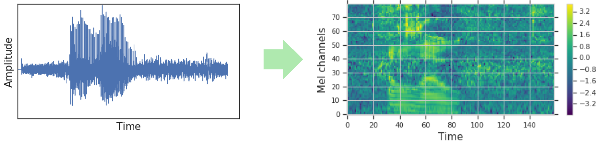 An audio waveform transformed into a log mel spectrogram. Image credit: Google AI is obviously making more news this week. Google scientists have recently developed a new “visual” approach to data augmentation in speech recognition, achieving interesting results. In many neural network applications, such as image classification, data augmentation is used to increase the amount of available training data. In speech recognition this traditionally involves deforming the audio waveform by speeding it up, slowing it down, or adding background noise. The new approach, instead, treats audio data augmentation as a visual problem. First, the audio waveform is transformed into a visual representation called a “log mel spectrogram”, which is a graph where the Y-axis represents “mel channels” (based on the “mel scale”, a perceptual scale of pitches) and color shades represent amplitude. Then modifications are applied to this visual representation, by masking slices of the graph on both axes. These augmentations have been chosen to help the network to be robust against deformations in the time direction, partial loss of frequency information and partial loss of small segments of speech of the input. Results obtained by Google scientists show that this approach allows to reach a lower Word Error Rate and prevents the network from over-fitting by giving it deliberately corrupted data. Google also pointed out that most of the work on automatic speech recognition in the past has been focused on looking for better networks, while this new work demonstrates that looking for better ways to train networks is a promising alternative direction of research. CMOS-based MEMS pioneer Nanusens seeks additional funding 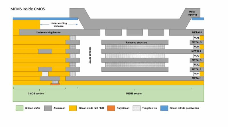 A MEMS built inside a CMOS structure. Image credit: Nanusens And in case you are planning to use a MEMS microphone to capture speech, you can expect a size reduction if the industry moves from MEMS to NEMS (Nano Electro Mechanical Systems). This is one of the promises of Nanusens, that has recently announced the opening of a new funding round on the crowdfunding platform CrowdCube. Launched at the MWC 2019 show in Barcelona, Spain, the UK-based company has developed a way to build MEMS sensors using the standard layer-by-layer CMOS process. In this approach, mechanical structures are sculpted by etching away silicon dioxide surrounding them. Nanusens points out that this is very hard to obtain because the CMOS process was never designed for this purpose. Once released from the surrounding silicon oxide, mechanical structures become sensitive to stress and so distort, which makes them useless. Nanusens has spent years researching and perfecting structure designs that do not distort when released. According to the company, up until now MEMS have required specially developed production processes, which prevent quick production ramp-up and cost reductions. Using a standard CMOS process allows high volume production, lower cost and a progressive size reduction of devices, thus moving from MEMS to NEMS. Renesas touch-key MCUs allows sensorless detection of various materials While MEMS are getting smaller, other types of sensors could disappear altogether. Sensorless detection of various materials is possible, in certain cases, using electrodes connected to the Renesas' RX130 capacitive touch-key microcontrollers. Besides sensing the presence of fingers on touch-keys, these MCUs can also be used to detect the presence or absence of powder, liquids or materials such as paper. Detection is obtained by measuring the capacitance between electrodes. According to Renesas, replacing the sensors with this electrode approach contributes to lower bill of materials (BOM) costs while enabling detection at multiple points using a single chip. This allows industrial equipment, office automation equipment, and home appliance manufacturers to explore detection systems for cost-constrained applications. Drone delivery receives FAA certification 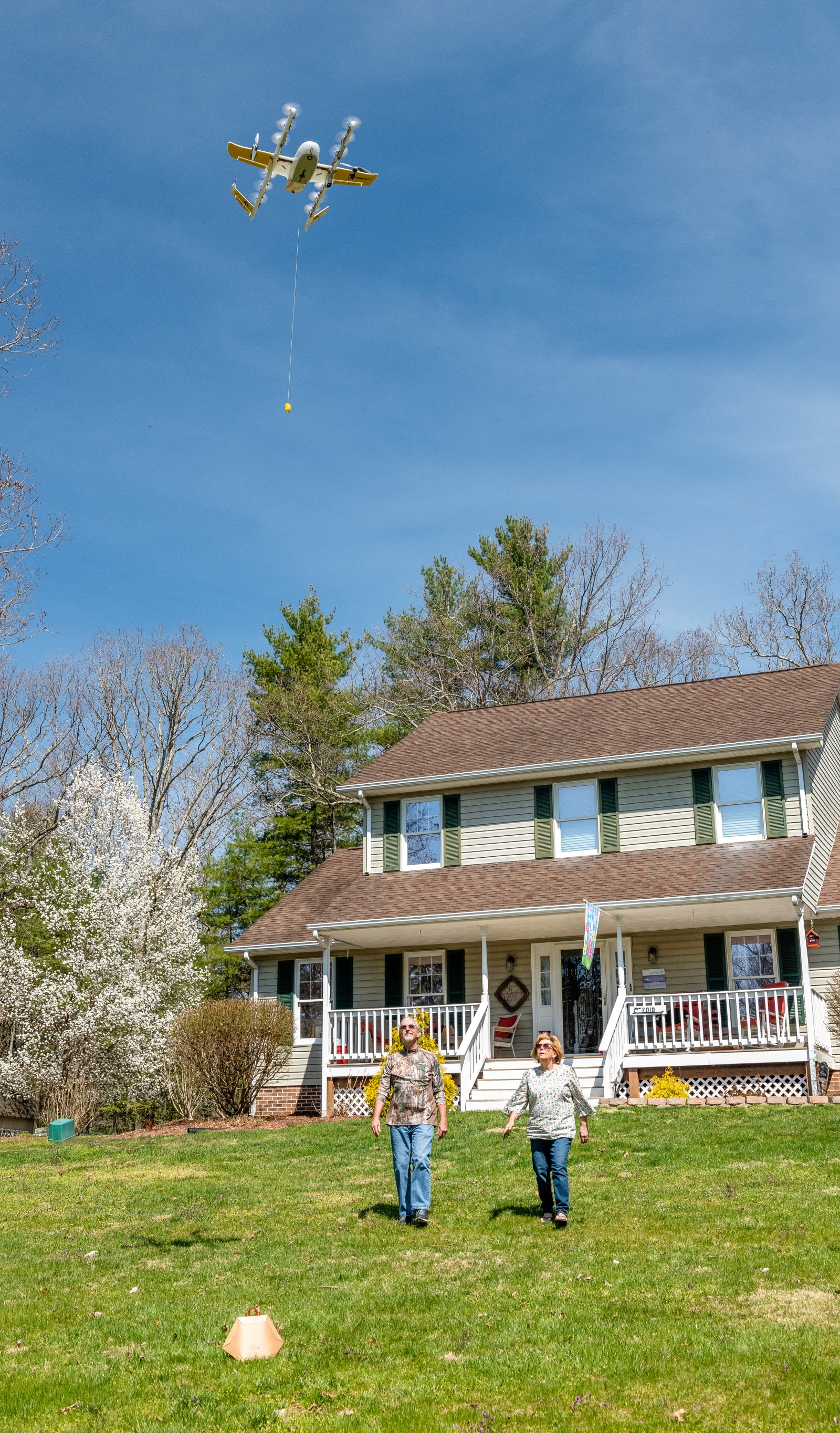 Drone delivery. Image credit: Wing Waiting for the express courier to deliver your MCU samples? Look up in the sky: the much-anticipated done delivery is becoming a reality. Wing, a startup owned by Google’s parent company Alphabet, achieved a significant milestone on April 23rd, becoming the first drone delivery company to receive Air Carrier Certification from the United States Federal Aviation Administration (FAA). Air Carrier Certification means that Wing can begin a commercial service delivering goods from local businesses to homes in the United States. FAA certification required the company to submit evidence that its operations are safe. These submissions included data showing that a delivery by Wing carries a lower risk to pedestrians than the same trip made by car. For the next several months, the company will be reaching out to businesses and community members in two Virginia towns (Blacksburg and Christiansburg) to demonstrate its technology, with the goal of launching a delivery trial later this year. Category: EDACafe Editorial |
|
|
|||||
|
|
|||||
|
|||||


 Animation, 3D Art and 3D Models")