EDACafe Editorial Roberto Frazzoli
Roberto Frazzoli is a contributing editor to EDACafe. His interests as a technology journalist focus on the semiconductor ecosystem in all its aspects. Roberto started covering electronics in 1987. His weekly contribution to EDACafe started in early 2019. Major stories this week: 5nm process node, MIT innovations, Power-on-Package, 1M-neuron chipApril 19th, 2019 by Roberto Frazzoli
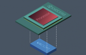
The five nanometer process node is here: on April 15, Samsung announced that its 5nm FinFET process technology – based on extreme ultraviolet lithography – is complete in its development and is now ready for customers’ samples. Compared to 7nm, the new process provides up to a 25 percent increase in logic area efficiency with 20 percent lower power consumption or 10 percent higher performance, still allowing reuse of all the 7nm intellectual property. Object-based data compression But advancing electronics is not just about scaling down to the next process node; research shows that many important aspects of data processing offer significant optimization opoortunities. Among them is data compression, aimed at reducing the frequency and amount of data fetched from main memory. In a paper presented at the ACM International Conference on Architectural Support for Programming Languages and Operating Systems this week, researchers from the Massachusetts Institute of Technology describe the first approach to compress ‘objects’ across the memory hierarchy, matching the characteristics of object-oriented programming. As MIT explained in a news release, traditional compression techniques operate on fixed-size chunks of data, and therefore handle objects poorly. The researchers overcame this limitation through their prior work that reorganizes the memory architecture to directly manipulate objects, as opposed to traditional cache-based structures. The new technique uncovers more compression opportunities as it leverages redundancy across objects, while the traditional ones were limited to finding redundancy within each fixed-size block. In experiments using a modified Java virtual machine, the new technique compressed twice as much data and reduced memory usage by half over traditional cache-based methods. Datacenter innovations: new SSD architecture, wafer-scale MEMS-based photonic switch Other optimizations can apply to storage in datacenters. This innovation, again, comes from the Massachusetts Institute of Technology and has been presented at the above-mentioned ACM conference. Called LightStore, it consists in a new storage architecture that uses modified Flash SSDs directly connected to the datacenter’s network. As MIT explains in a news release, optimization opportunities comes from the fact that so far Flash SSDs have been plugged in to replace old hard disks without changing anything else in the datacenter architecture. In the new solution, instead, Flash SSDs have been modified to be accessed in terms of ‘key-value pairs’; the flash management software has also been changed to make it computationally light. The researchers then designed an ‘adapter’ software, also computationally light, which translates all user requests from app services into key-value pairs. In experiments, the MIT team found that a cluster of four LightStore units ran twice as efficiently as traditional storage servers, measured by the power consumption needed to field data requests. The cluster also required less than half the physical space occupied by existing servers. Another innovation aimed at datacenters comes from the Berkeley University, where researchers have created a new 240-by-240 silicon photonic switch, built with more than 50,000 MEMS light switches. As the team explained in an article on the journal Optica, in the past decade the port counts of silicon photonic switches have increased steadily to 128×128, but further scaling is constrained by the maximum reticle size (2–3 cm) of lithography tools. To overcome the die size limit, the Berkeley researchers used wafer-scale integration, and – as a proof of concept demonstration – they fabricated a 240×240 switch by lithographically stitching a 3×3 array of identical 80×80 switch blocks across reticle boundaries. The resulting switch exhibits low signal loss and high switching speed. Feeding power-hungry CPUs and GPUs With compute-intensive applications such as AI, today’s high-performance CPUs and GPUs are absorbing currents in the hundreds of ampere range. Point-of-Load power architectures mitigate power distribution losses on the motherboard, but the remaining short distance to the processor – the ‘last inch’, consisting of motherboard conductors and interconnects within the processor socket – has become a limiting factor in performance and total system efficiency. The Power-on-Package solution recently developed by Vicor eliminates the last inch by placing the voltage regulator inside the processor package. Delivering 48V to the processor socket obviously allows a dramatic reduction of current delivery, thus reducing power losses and minimizing the number of pins needed for power, so that more pins can be used for I/Os. Now a collaboration between Kyocera and Vicor aims to maximize performance for the Power-on-Package solution and minimize its time-to-market for emerging processor technologies. Collaboration will focus on the latest version of the solution, called Vertical Power Delivery (VPD), that provides power from the bottom side of the processor. Low power vision processing with a 1 million neuron chip But AI processing does not have to be a power-hungry application, according to companies making neuromorphic chips. Among them is aiCTX, based in Zurich, Switzerland. The company, that recently received a USD 1.5M pre-A investment from Baidu Ventures, develops dedicated event-driven neuromorphic processors for real-time vision processing. On April 14 aiCTX announced DynapCNN, a new fully-asynchronous event-driven neuromorphic AI processor for ultra-low power, always-on, real-time applications. DynapCNN, fabricated in 22nm technology, houses over 1 million spiking neurons and 4 million programmable parameters, with a scalable architecture suited for implementing Convolutional Neural Networks. According to aiCTX, DynapCNN is 100–1000 times more power efficient than the state of the art, and delivers 10 times shorter latencies in real-time vision processing. Computation in DynapCNN is triggered directly by changes in the visual scene, without using a high-speed clock. DynapCNN’s continuous computation enables a latency of below 5ms, at least a 10x improvement from the current deep learning solutions available in the market for real-time vision processing. Natural language understanding at the edge Other recent developments in the AI arena include bringing natural language understanding to the edge. On April 18, Sensory (Santa Clara, CA) announced the first full feature release of TrulyNatural, the company's embedded large vocabulary speech recognition platform. The solution does not require any data to leave the device (no Internet connection), thus eliminating the privacy concerns associated with sending voice data to the cloud. According to Sensory, TrulyNatural is an order of magnitude smaller than open source options without sacrificing performance. Category: EDACafe Editorial |
|
|
|||||
|
|
|||||
|
|||||


