Archive for the ‘Uncategorized’ Category
Tuesday, January 4th, 2022
Note: Here’s another Q&A post I did for the SEMI blog. In this interview, I talk with John Lee, Rich Goldman and Marc Swinnen of Ansys.
Spend any time with Ansys’ John Lee, Rich Goldman or Marc Swinnen and you’ll hear plenty of optimism about the semiconductor industry even though they tick off a long list of looming design challenges. The need for reliable and effective electronic systems, they emphasize, is great and runs through high tech, aerospace and defense, automotive, IoT and 5G with communications being a common denominator.
The three are especially bullish these days on changing market dynamics brought on by systems companies building company-specific bespoke, or custom, silicon. These systems companies are building chips with a different perspective and a fresh look at silicon design, a move away from the more traditional segment-specific silicon due to much more complexity.
Ansys, a member of the ESD Alliance, a SEMI Technology Community, is a 4,100-employee company with a comprehensive portfolio of multiphysics engineering simulation software for product design, testing and operation products and services. John, Rich, Marc and I focused on Ansys’ semiconductor and electronics segment for our conversation.
(more…)
No Comments »
Thursday, December 9th, 2021
Note: This Q&A interview I did with Jean-Marie Brunet, senior director of marketing, product management and product engineering at Siemens EDA, in July continues my blog post series with member company executives that appears on the SEMI website.
 In the span of a few short months earlier this year, Mentor Graphics became Siemens EDA and introduced a suite of integrated hardware-assisted verification tools, the first product launch under the new Siemens EDA brand. In the span of a few short months earlier this year, Mentor Graphics became Siemens EDA and introduced a suite of integrated hardware-assisted verification tools, the first product launch under the new Siemens EDA brand.
Jean-Marie Brunet, senior director of marketing, product management and product engineering at Siemens EDA, orchestrated the launch and connected with me for a discussion about the chip design verification space. As he pointed out, verification and validation of systems is a fast-growing and important market segment to the electronic system design ecosystem.
Smith: What trends do you see in chip design? What is driving these trends?
Brunet: Chip verification costs continue to grow faster than design costs because of factors such as increasing design complexity, rising computing power, surging I/O traffic activity, increasing energy consumption and the widespread use of peripherals. These dynamics are being driven by new data center networking, communications/5G, autonomous driving, artificial intelligence (AI) and machine learning (ML), and storage applications.
These trends also indicate the need for more powerful verification tools and expanded verification objectives that include power and performance analysis. Hardware-assisted verification tools are perfect for meeting these demands.
(more…)
No Comments »
Tuesday, November 30th, 2021
Note: Last week, I post the first of my Q&A blog post series with ESD Alliance member company executives that appears on the SEMI website. This Q&A features Adnan Hamid of Breker Verification who describes the functional verification space.
 Adnan Hamid, CEO, founder and visionary of Breker Verification Systems, an ESD Alliance member based in San Jose, Calif., once described his job in chip design verification at AMD as “breaking things.” When it came to naming his startup, Breaker was a natural choice. After some consideration, the “a” was dropped and the company became Breker. Now Hamid is breaking the most complex semiconductor designs and Breker, moving from a startup to a scale-up company, is a noted part of the functional verification space. Adnan Hamid, CEO, founder and visionary of Breker Verification Systems, an ESD Alliance member based in San Jose, Calif., once described his job in chip design verification at AMD as “breaking things.” When it came to naming his startup, Breaker was a natural choice. After some consideration, the “a” was dropped and the company became Breker. Now Hamid is breaking the most complex semiconductor designs and Breker, moving from a startup to a scale-up company, is a noted part of the functional verification space.
Smith: Why does verification continue to take the most amount of time in a project cycle?
Hamid: The project cycle for semiconductor design has changed. Design abstraction has been raised to a much higher level than the days when developers were connecting logic gates. Today’s developers are typing functions that don’t include lower-level implementation details. Designs incorporate more blocks of reusable IP. Both reduce design time.
Meanwhile, designs are getting bigger with more blocks of IP stitched together, all in need of testing. As design complexity grows, the amount of testing and verification increases as a square of design effort. One block requires one functional verification effort. Four blocks of IP mean up to 16 functional interactions require verification.
While design is moving up the abstraction level, that’s not the case for verification, where plenty of detail must be reimplemented. Verification has certainly evolved, but engineers still think at the level of independent stimulus, response and coverage, driving the need to allocate so much time for verification.
(more…)
No Comments »
Thursday, November 18th, 2021
Note: This question-and-answer blog post I did with Aki Fujimura, CEO of D2S and a member of the ESD Alliance Governing Council, first appeared on the SEMI website in May. It also kicked-off my Q&A blog post series with member company executives.
A change is underway in the manufacturing sector as the use of curvilinear shapes on photomasks grows, leading to the real possibility of curvilinear shapes in designs. It may just be the start of a revolution away from Manhattan or rectangular shapes to curvilinear shapes. Changing the physical design infrastructure to be curvilinear seems too daunting a task. Are curvilinear shapes in designs a real possibility?
 Aki Fujimura I turned to Aki Fujimura, CEO of D2S and a member of the ESD Alliance Governing Council, to further explain the shape of the future.
Fujimura: Manufactured masks and wafers are all curvilinear, even if the input CAD geometries are rectilinear (shown in Figure 1). It’s always been true that nature can’t make 90-degree turns, so sharp corners were always a matter of how closely you looked. These days, at the leading-edge nodes and their required resolutions, wafers and even masks are all visibly curvilinear as you can see in the graphic on the left in Figure 2.
Since the 1980s, both chip design and chip manufacturing systems have used axis-aligned rectangles, or “Manhattan” geometries, because 1) that was sufficient to design transistors and interconnect for the most part, and 2) CPU-based computer algorithms can be made much more efficient for Manhattan geometries. Curvilinear shapes can be piecewise linear polygons of some resolution, or spline-like formats that are curvilinear at any resolution, or specific curved patterns like circles and ovals.

Figure 1: All shapes on masks and wafers are curvilinear, even if the input geometries are Manhattan. Source: D2S
(more…)
No Comments »
Tuesday, October 19th, 2021
 It’s with great pleasure that I’m able to announce Maheen Hamid, Chief Operating Officer and Chief Financial Officer of Breker Verification Systems, is now a member of the Electronic System Design Alliance Governing Council. It’s with great pleasure that I’m able to announce Maheen Hamid, Chief Operating Officer and Chief Financial Officer of Breker Verification Systems, is now a member of the Electronic System Design Alliance Governing Council.
 Maheen Hamid Maheen, a seasoned, accomplished executive, assumes the seat formerly held by Babak Taheri who was CEO/CTO of Silvaco. She brings more than 15 years of financial experience in deal structuring and operations management in diverse industries including wireless telecommunications, clean energy, health, and infrastructure projects in emerging markets. Prior to Breker, Maheen served in various roles in investment banking and management consulting and is an occasional contributor to different business journals and forums covering a broad range of topics related to management. She holds a BBA from North South University in Bangladesh and an MBA from the University of Texas at Austin.
“I am delighted to be joining the governing council of this important organization at a key moment in its history,” Maheen is quoted as saying in the news release announcing her appointment. “As Breker has grown to become an established EDA company working with semiconductor companies in the area of test suite synthesis, we have gained a wealth of experience and I hope to bring this perspective to the council.”
Maheen will serve a two-year term that runs through 2023, along with:
- Aart de Geus, chairman and co-CEO of Synopsys, Inc.
- Dean Drako, president and CEO at IC Manage
- Aki Fujimura, D2S’ CEO
- John Kibarian, president and CEO of PDF Solutions, Inc.
- Prakash Narain, president and CEO from Real Intent
- Joe Sawicki, executive vice president of Siemens EDA
- Simon Segars, CEO of Arm, who serves as the Governing Council Chair
- Bob Smith, executive director of the ESD Alliance
Many readers know Breker Verification Systems as a chip design verification company founded in 2003 by Maheen and her husband Adnan Hamid. Specially, it provides Portable Stimulus solutions, a standard means to specify verification intent and behaviors reusable across target platforms.
(more…)
No Comments »
Thursday, October 14th, 2021
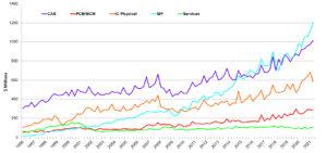
 We did it again! The electronic system design (ESD) ecosystem reported a revenue increase of 14.6% year-over-year from $2,783.9 million to $3,191.4 million in Q2 2021. Our latest Electronic Design Market Data (EDMD) report comparing the most recent four quarters to the prior four also found that the four-quarter moving average rose 15.5%, the highest annual growth since 2011. We did it again! The electronic system design (ESD) ecosystem reported a revenue increase of 14.6% year-over-year from $2,783.9 million to $3,191.4 million in Q2 2021. Our latest Electronic Design Market Data (EDMD) report comparing the most recent four quarters to the prior four also found that the four-quarter moving average rose 15.5%, the highest annual growth since 2011. 
According to Wally Rhines, executive sponsor of the SEMI EDMD report, double-digit growth was reported in Computer Aided Engineering (CAE), Printed Circuit Board and Multi-Chip Module (PCB and MCM), Semiconductor IP (SIP) and Services. In addition, all geographic regions reported growth on a rolling four-quarter basis, with the Americas; Asia Pacific (APAC); and Europe, Middle East, and Africa (EMEA) showing a substantial year-over-year increase.
It also tracks total employment at participating companies. In the latest report, companies employed 49,964 people globally in Q2 2021, a 7.3% increase over the Q2 2020 headcount of 46,579 and up 1.9% compared to Q1 2021.
(more…)
No Comments »
Thursday, October 7th, 2021
 I’m pleased to welcome Aselta Nanographics and Metis Microsystems to the ESD Alliance community. Both have countless reasons for joining. For example, Yorick Trouiller, Aselta Nanographics’ CEO, noted: “Joining the ESD Alliance is a great opportunity to stay connected with the EDA community and take an active part in the discussions driving the future of semiconductor manufacturing.” I’m pleased to welcome Aselta Nanographics and Metis Microsystems to the ESD Alliance community. Both have countless reasons for joining. For example, Yorick Trouiller, Aselta Nanographics’ CEO, noted: “Joining the ESD Alliance is a great opportunity to stay connected with the EDA community and take an active part in the discussions driving the future of semiconductor manufacturing.”
According to Azeez Bhavnagarwala, founder of Metis Microsystems, “As a startup dedicated to enabling energy efficiency in semiconductor products, we are excited about the opportunities the ESD Alliance and SEMI offer to connect with the network of industry members. Both the ESD Alliance and SEMI have initiatives and resources offered by their domain-specific Smart Initiatives, Technology Communities and Committees that can help us understand and engage with industry members as a startup on topics of common interest.”
 Our New Members Our New Members
Aselta Nanographics of Grenoble, France, provides advanced software solutions for wafer and mask patterning based on e-beam technology. It develops software tools to improve the quality process of chip production and operates in the IC manufacturing world providing advanced software solutions for wafer and mask patterning based on e-beam technology as well as solutions for contour-based metrology. Aselta Nanographics is a spin-off of CEA-Leti and maintains strong links with cutting-edge fundamental research and applies it to deliver advanced industrial solutions to customers in the U.S., Europe and Asia.
(more…)
No Comments »
Tuesday, September 7th, 2021
I take pride in being able to announce completion of the year-long joint development effort of the anti-piracy server certification protocol for software license management led by the ESD Alliance. The initiative was approved by development committee members Cadence, Siemens EDA and Synopsys who recognize the high cost of software piracy costs hurts both vendors and their customers, a problem the protocol will help mitigate.
The SEMI Server Certification Protocol (SSCP) offers protection against software piracy. It addresses this problem by uniquely identifying each customer license server to assure that licenses are issued only by authorized servers. SCCP, now undergoing standardization, will be managed by SEMI’s Standards Group after its finalization as an industry standard. Committee members intend to implement the protocol in their respective license management software.
Credit for this achievement goes to Cadence, Siemens EDA and Synopsys committee members as well as SEMI for their work to reach this milestone and the effort continues as we move forward to finalize SSCP as an industry standard. An industry-standard protocol to combat software piracy is a growing necessity for design automation software suppliers to ensure only authorized servers are issuing licenses. Design automation software is complex and requires ongoing and significant R&D investments. Bad actors can apply server cloning techniques to access unlicensed copies of the software, putting legitimate users at a competitive disadvantage and potentially forcing software vendors to increase prices to support continuing investments in R&D.
(more…)
No Comments »
Tuesday, August 17th, 2021
 Larry Disenhof We’re switching gears after the two-part, work-from-home panel series we co-hosted with Accellera to focus on export compliance with Larry Disenhof, Chair of our Export Committee and Group Director in Cadence’s Government and Trade Compliance Group.
As Larry will explain, the world of export compliance is increasingly complex and perplexing. During “Understanding Export Regulations Affecting the Electronic System Design Ecosystem” webcast Wednesday, September 15, he will offer his perspective and insight into today’s export climate and offer ways to navigate export regulations.
Larry is an expert with more than 20 years of experience representing the electronic system design ecosystem to export administration agencies. His unique position makes him well qualified to provide historical context, understanding of current controls and potential new controls affecting electronic system design software and technologies.
A bit about our Export Committee is in order here. Under Larry’s leadership, the Export Committee is a valued resource for our members. The committee represents the electronic system design ecosystem in Washington, D.C., with agencies overseeing export regulations and other regulatory organizations. Its goal is to educate government agencies about our products and how they are classified in the Commerce Control List to ensure the correct level of export controls are applied.
(more…)
No Comments »
|


